A kind of preparation method of cadmium manganese telluride crystal transmission electron microscope section sample
A technology of transmission electron microscopy and cadmium telluride manganese, which is applied in the field of compound semiconductor materials, can solve the problems that affect the analysis of the real structure and defects of materials, low success rate, and waste of time
- Summary
- Abstract
- Description
- Claims
- Application Information
AI Technical Summary
Problems solved by technology
Method used
Image
Examples
preparation example Construction
[0029] The present invention uses a hand-held wedge polisher for the preparation of a TEM cross-sectional sample of a vanadium-doped cadmium telluride manganese crystal, and the technical solution adopted to solve the technical problem: a preparation method of a cadmium telluride manganese TEM sample, its characteristics It consists of the following steps:
[0030] (1): Polish the first side of the sample
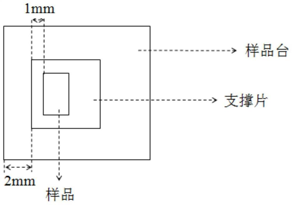
[0031] Including fixing the cadmium manganese telluride TEM sample to be polished on the sample stage, the plane where the sample is located is coplanar with the other two support rods, and polishing the cadmium manganese telluride TEM sample with 9 μm diamond film, 3 μm diamond film and 1 μm diamond film in sequence first side. The basis for replacing the diamond film is: when the surface of the sample is polished to only the same direction scratches left by the diamond film particles in the previous step, replace the film of the next specification. Get the cadmium manga...
Embodiment 1
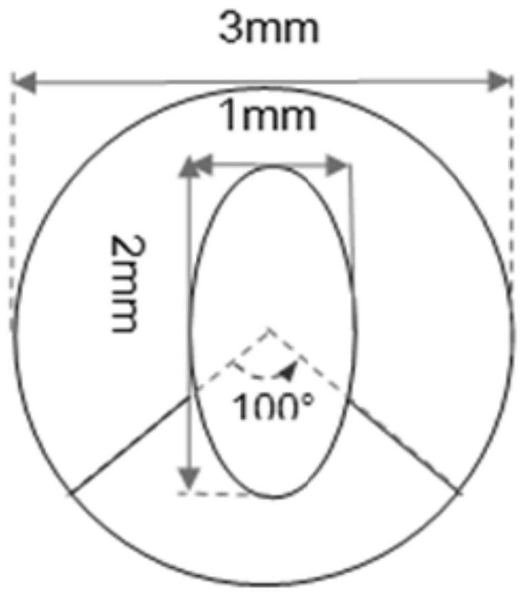
[0057] On the first day, grind the first side of the CMT sample: use ultrasonic or blade to remove Cd 0.9 mn 0.1 The Te:V sample was cut into a rectangular sample of 3mm×2mm, hereinafter referred to as the CMT sample. Remove the sample stage of the polisher produced by Allied HighTech., put it on a heating stage with a set temperature of 120°C, fix the CMT sample on the sample stage with crystal adhesive glue, and wait for 10 minutes after the sample is firmly adhered. Polish the sample with 9μm, 3μm and 1μm diamond grinding films in turn. Every time the film is replaced, it is necessary to confirm that the scratches are consistent in a certain direction under a 50x optical microscope, indicating that the scratches are caused by the diamond film in the previous step rather than other scratches. mark. Then remove the CMT sample, wash it carefully with acetone solution, and replace the acetone solution 2 to 3 times.
[0058] Adhesive support material gallium arsenide: use the...
PUM
| Property | Measurement | Unit |
|---|---|---|
| Knoop hardness | aaaaa | aaaaa |
Abstract
Description
Claims
Application Information


