A manufacturing method of an array substrate

A technology for array substrates and manufacturing methods, which is applied in the field of array substrate manufacturing, and can solve problems such as molybdenum metal residues and less wet etching time

Active Publication Date: 2018-12-28
SHENZHEN CHINA STAR OPTOELECTRONICS SEMICON DISPLAY TECH CO LTD
View PDF8 Cites 2 Cited by
  • Summary
  • Abstract
  • Description
  • Claims
  • Application Information

AI Technical Summary

Problems solved by technology

[0005] The invention provides a method for manufacturing an array substrate to solve the problem of molybdenum metal residue due to less wet etching time for metal lines during the preparation of the array substrate

Method used


Image

  • A manufacturing method of an array substrate
  • A manufacturing method of an array substrate
  • A manufacturing method of an array substrate

Examples


Embodiment Construction

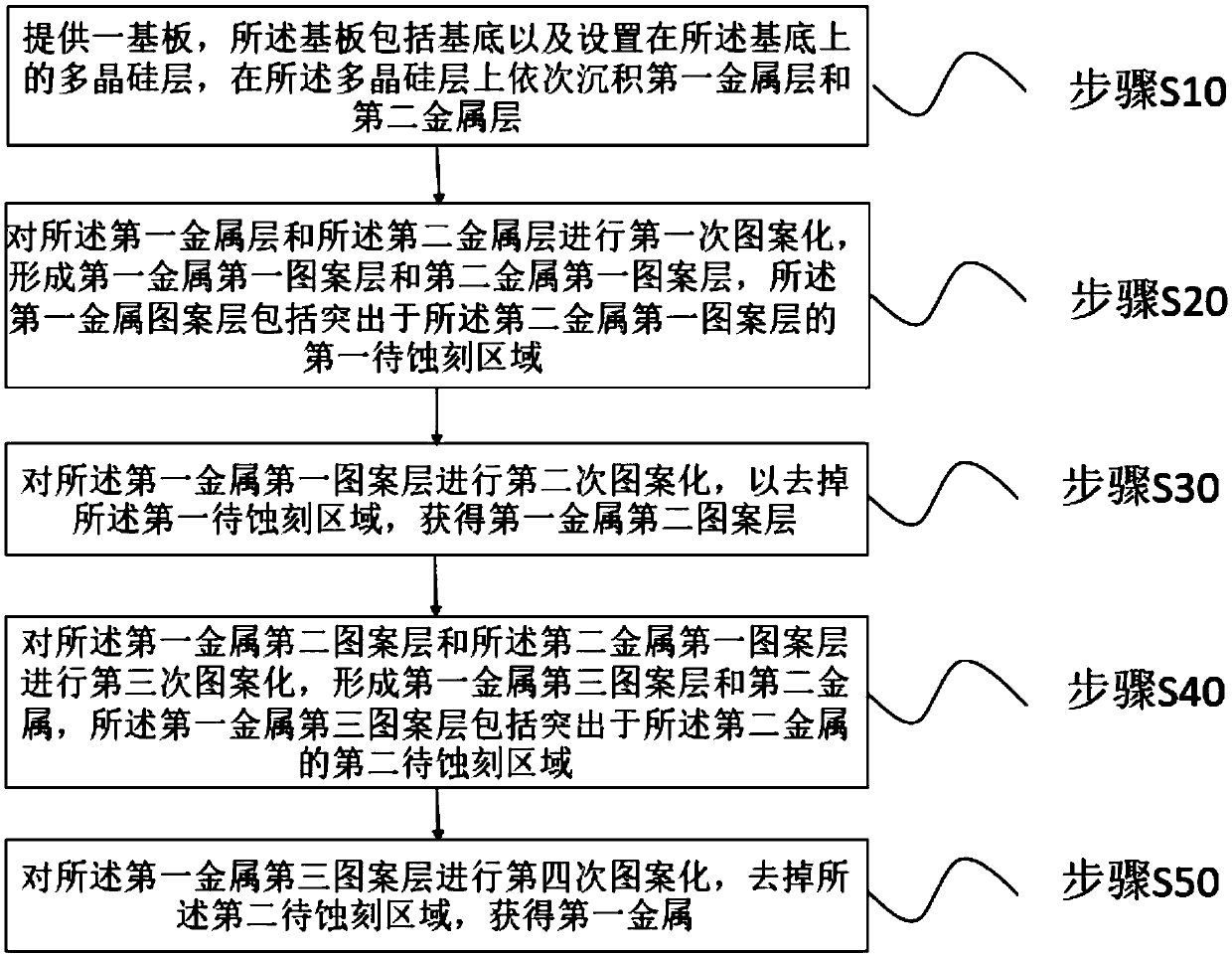
[0038] The following descriptions of the various embodiments refer to the accompanying drawings to illustrate specific embodiments in which the invention may be practiced. The directional terms mentioned in the present invention, such as [top], [bottom], [front], [back], [left], [right], [inside], [outside], [side], etc., are only for reference The orientation of the attached schema. Therefore, the directional terms used are used to illustrate and understand the present invention, but not to limit the present invention. In the figures, structurally similar elements are denoted by the same reference numerals.

[0039] The present invention provides a method for manufacturing an array substrate to solve the problem of molybdenum metal residue due to less wet etching time for metal lines during the preparation process of the array substrate, and this embodiment can improve this defect.

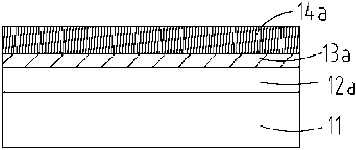
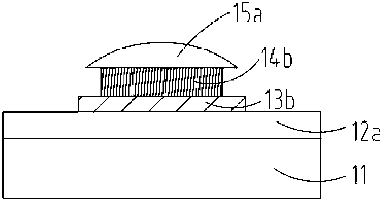
[0040] figure 1 is a schematic flow chart of a method for fabricating an array substrate i...


PUM

PropertyMeasurementUnit
thicknessaaaaaaaaaa

Abstract

The invention provides a manufacturing method of an array substrate, comprising the following steps: providing a substrate, wherein the substrate comprises a substrate and a polysilicon layer arrangedon the substrate; depositing a first metal layer and a second metal layer on the polysilicon layer sequentially; depositing a second metal layer on the polysilicon layer sequentially; performing a first patterning, the second metal layer including a first region to be etched protruding from the third metal layer; performing a second patterning to remove a first region to be etched of the second metal layer; performing a third patterning, the second metal layer including a second region to be etched protruding from the third metal layer; performing a fourth patterning to remove the second region to be etched of the second metal layer. By adopting the dry etching method to remove the residual metal molybdenum in the metal line, the invention can reduce the risk of metal molybdenum residue while reducing the wet etching time of the metal line, thereby avoiding the wire breakage problem caused by the excessively thin metal line width.

Description

technical field [0001] The invention relates to the display field, in particular to a method for manufacturing an array substrate. Background technique [0002] In high-generation display panels, copper material has gradually become a substitute for traditional aluminum material in metal lines due to its advantages of low impedance. [0003] The thickness of the existing copper wires is usually 3000 angstroms, but with the increase of the size of the display panel and the improvement of the resolution, the traditional copper wires are gradually difficult to solve other problems such as phase circuit delay. The usual solution is to increase the thickness of the copper wires. thickness. [0004] In the preparation process of copper wire, the etching time of copper wire in the wet etching process will increase due to the increase of thickness, which will cause the line width of copper wire to be too thin, which will increase the risk of copper wire disconnection; if the wet et...

Claims


Application Information

Patent Timeline
Patent Type & Authority Applications(China)
IPC IPC(8): H01L21/77
CPCH01L27/1259H01L21/32135H01L21/32134H01L29/66757H01L27/124
Inventor 陈梦
Owner SHENZHEN CHINA STAR OPTOELECTRONICS SEMICON DISPLAY TECH CO LTD
Why Eureka
Try Eureka