Microelectronic die

A technology of microelectronics and tube cores, which is applied in the direction of circuits, electrical components, electric solid devices, etc., can solve the problems of limited magnetic interference processing effect, achieve broad market prospects and application prospects, and reduce the effect of magnetic interference

Inactive Publication Date: 2019-01-08
安徽星宇生产力促进中心有限公司
View PDF10 Cites 0 Cited by
  • Summary
  • Abstract
  • Description
  • Claims
  • Application Information

AI Technical Summary

Problems solved by technology

[0004] The analysis found that there is magnetic interference among the adjacently arranged microelectronic die cores, and the pure filling material has limited effect on dealing with magnetic interference, and there are aspects to be improved

Method used


Image

  • Microelectronic die
  • Microelectronic die
  • Microelectronic die

Examples


Embodiment Construction

[0018] The following will clearly and completely describe the technical solutions in the embodiments of the present invention with reference to the accompanying drawings in the embodiments of the present invention. Obviously, the described embodiments are only some, not all, embodiments of the present invention. Based on the embodiments of the present invention, all other embodiments obtained by persons of ordinary skill in the art without making creative efforts belong to the protection scope of the present invention.

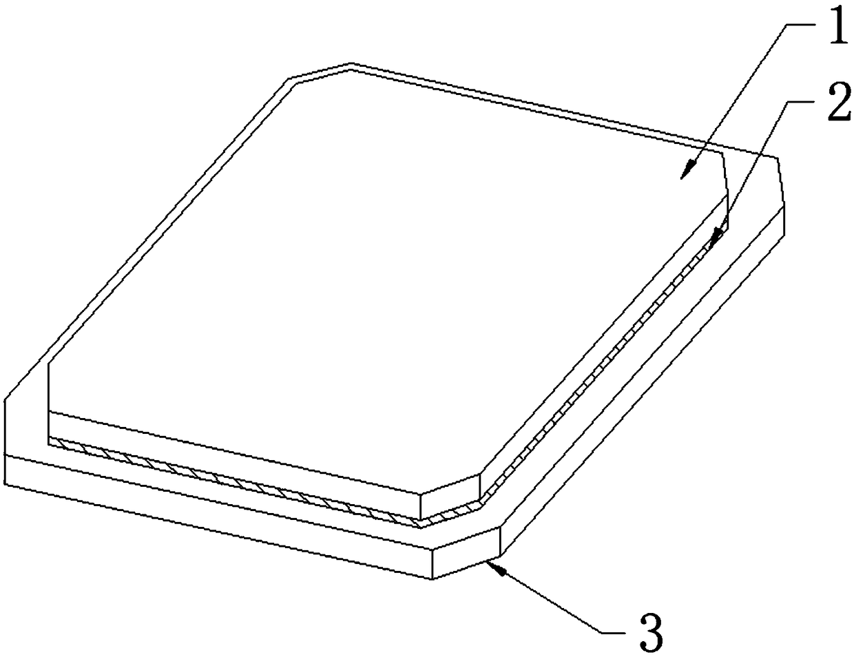
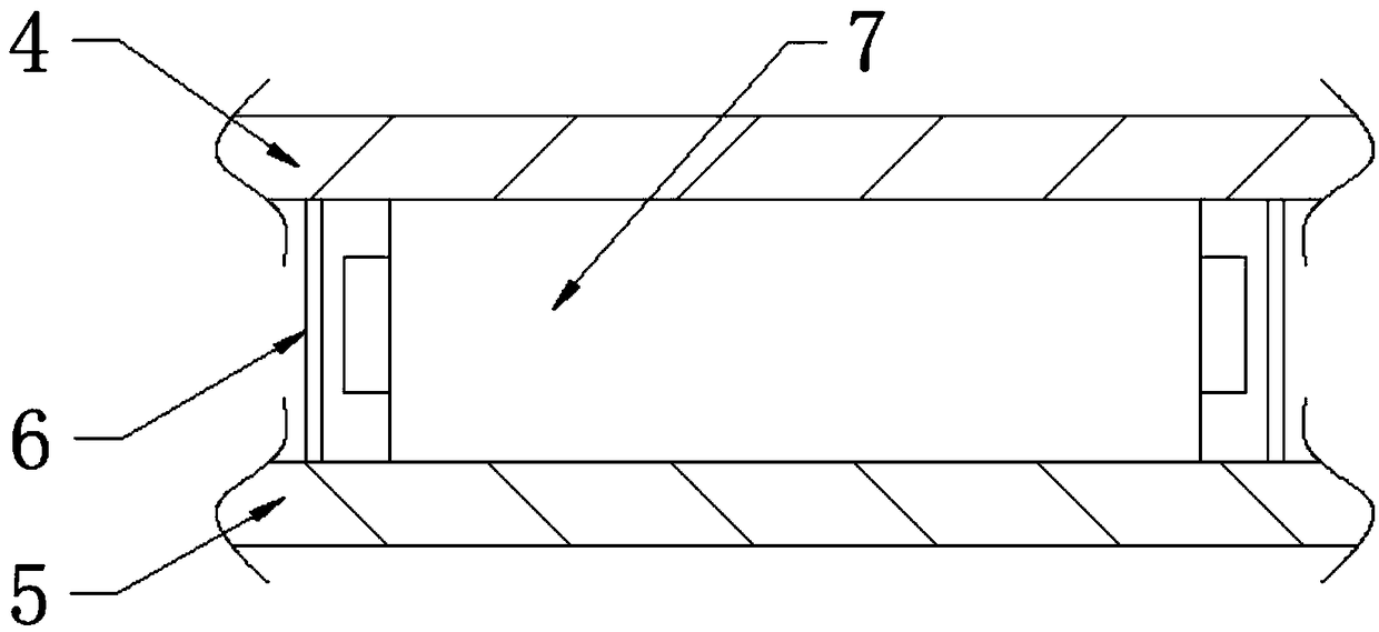
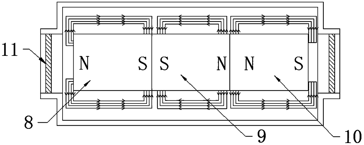
[0019] see Figure 1-3 , the present invention provides a technical solution: a microelectronic die, comprising a die body 1, the die body 1 is composed of an active surface 4 and a substrate 5, the active surface 4 is arranged on the substrate 5, and the middle position of the active surface 4 and the substrate 5 is provided with a magnetic shield 7, the active surface 4 and the substrate 5 are fixedly connected with the magnetic shield 7, the magnetic shield...


PUM


Abstract

A microelectronic die include a die body, the die body is composed of an active surface and a substrate, the active surface is arranged on the top of the substrate, The active surface and the substrate are fixedly connected with the magnetic shielding cover, the outer side of the magnetic shielding cover is filled with a filling material, and the inside of the magnetic shielding cover is respectively provided with a first magnet, a second magnet and a third magnet arranged in a slotted manner. According to the invention, A magnetic field of a plurality of magnetic inductance line with oppositepolarity is generated by a plurality of magnet, and according to the difference of the magnetic conductivity of the magnetic fields, that magnetic inductance lines of external magnetic interference are refracted on an intersection surface between the magnetic inductance lines, thus, the magnetic interference between the die arrangement can be reduced, and the microelectronic die has significant practical advantages, and has broad market prospects and application prospects.

Description

technical field [0001] The invention relates to the technical field of dies, in particular to a microelectronic die. Background technique [0002] The so-called die refers to the chip used to manufacture integrated blocks in integrated circuits. The circuit composed of tens to tens of thousands to N number of electronic components is called an integrated circuit. The chip of this integrated component is the die of the integrated circuit. [0003] After retrieval, the patent No. CN104465568B discloses a stacked microelectronic die embedded in a microelectronic substrate, which is achieved by including at least one first microelectronic die attached to a second microelectronic die, wherein An underfill material is provided between the second microelectronic die and the at least one first microelectronic die. A microelectronic substrate is then formed by laminating the first microelectronic die and the second microelectronic die in the base material. [0004] The analysis fo...

Claims


Application Information

Patent Timeline
Patent Type & Authority Applications(China)
IPC IPC(8): H01L23/552
CPCH01L23/552
Inventor 吴胜松叶桂如吴胜琴
Owner 安徽星宇生产力促进中心有限公司
Why Eureka
Try Eureka