Array substrate and driving method thereof, and liquid crystal display device and driving method thereof

A technology of an array substrate and a driving method, applied in the field of liquid crystal display, can solve problems such as display unevenness, and achieve the effects of solving display unevenness, improving display image quality, and reducing signal coupling

Active Publication Date: 2019-01-11
KUSN INFOVISION OPTOELECTRONICS
View PDF33 Cites 3 Cited by
  • Summary
  • Abstract
  • Description
  • Claims
  • Application Information

AI Technical Summary

Problems solved by technology

[0006] In order to overcome the shortcomings and deficiencies existing in the prior art, the object of the present invention is to provide an array substrate and its driving method, a liquid crystal display device and its driving method, so as to solve the need of connecting the pixel electrodes and the data lines of two adjacent sub-pixels Different numbers of TFTs lead to uneven display

Method used


Image

  • Array substrate and driving method thereof, and liquid crystal display device and driving method thereof
  • Array substrate and driving method thereof, and liquid crystal display device and driving method thereof
  • Array substrate and driving method thereof, and liquid crystal display device and driving method thereof

Examples


Embodiment 1

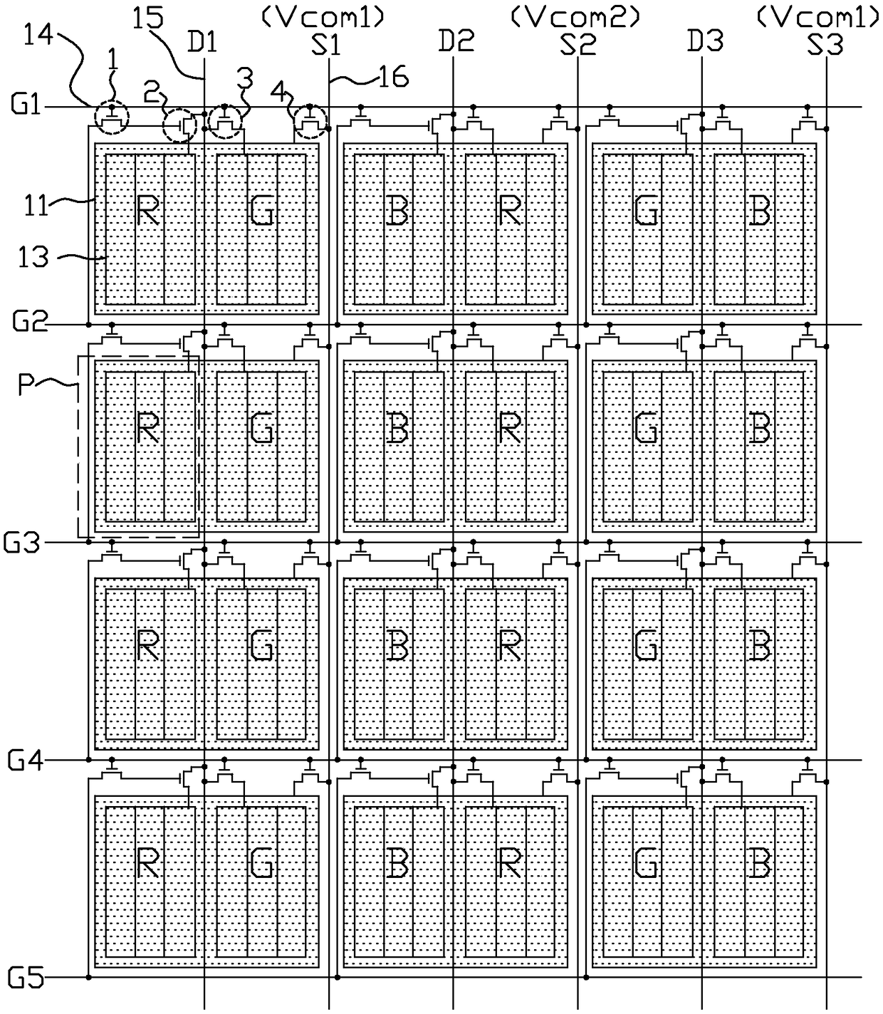
[0048] Such as image 3 with Figure 4 As shown, Embodiment 1 of the present invention provides an array substrate. The array substrate 10 is provided with a plurality of scanning lines 14 and a plurality of data lines 15. The plurality of data lines 15 and the plurality of common lines 16 extend in the same direction. A plurality of common lines 16 and a plurality of data lines 15 are alternately arranged in the direction of the scanning lines 14, every two adjacent data lines 15 and the common lines 16 are separated by the width of a column of pixel units P, and the array substrate 10 is composed of a plurality of scanning lines. The line 14 is insulated from and intersects with a plurality of data lines 15 and a plurality of common lines 16 to define a plurality of pixel units P, and each pixel unit P is provided with a pixel electrode 13 .

[0049] The array substrate 10 is also provided with a plurality of common electrode blocks 11 distributed in an array and insulated ...

Embodiment 2

[0064] Such as Figure 11 with Figure 12 As shown, the array substrate provided by Embodiment 2 of the present invention is the same as Embodiment 1 ( image 3 with Figure 4) are basically the same array substrate, the difference is that in this embodiment, the pixel electrode 13 in the first pixel unit P1 of each row of pixel units P is connected to the lower pixel electrode 13 through the first switching element 1 and the second switching element 2 The two scan lines 14 on the upper and lower sides of a row of pixel units P are connected.

[0065] Specifically, the pixel electrode 13 in the first pixel unit P1 of the pixel unit P in this row is connected to the two scanning lines 14 located on the upper and lower sides of the pixel unit P in the next row through the first switching element 1 and the second switching element 2. In this embodiment, the control terminal of the first switch element 1, the control terminal of the third switch element 3, and the control termi...

Embodiment 3

[0068] Such as Figure 13 As shown, the array substrate provided by Embodiment 3 of the present invention is the same as Embodiment 1 ( image 3 with Figure 4 ) are basically the same array substrate, the difference is that in this embodiment, a plurality of common lines 16 and a plurality of data lines 15 extend along the same direction, and each common electrode block 11 covers two adjacent pixel units P is a group, two adjacent groups of pixel units P are arranged in a repeating period in the direction of the scanning line 14, and two adjacent groups of pixel units P are connected with two data lines 15 and two common lines 16, wherein each data line The line 15 is arranged between two adjacent pixel units P in each group, and the two common lines 16 are arranged between two adjacent groups of pixel units P and are arranged side by side and adjacent to each other.

[0069] Those skilled in the art should understand that the remaining structures and working principles of ...


PUM


Abstract

The invention discloses an array substrate and a driving method thereof, and a liquid crystal display device and a driving method thereof. The array substrate is provided with a plurality of scanninglines, a plurality of data lines, and a plurality of pixel units, and further provided with a plurality of common lines and a plurality of common electrode blocks, wherein each common electrode blockcovers two adjacent pixel units at the same time. Pixel electrodes in a first pixel unit are connected to two adjacent scan lines and one data line through a first switching element and a second switching element. The first switching element has a control end connected to one scanning line, one conductive end of the first switching element is connected to the other scanning line, and another conductive end of the first switching element is connected to a control end of the second switching element. Two conductive ends of the second switching element are respectively connected to the pixel electrodes and the data lines. Pixel electrodes in a second pixel unit are connected to the adjacent scan lines and data lines through a third switching element. Each common electrode block is connected to the adjacent scan lines and the common lines through a fourth switching element.

Description

technical field [0001] The present invention relates to the technical field of liquid crystal display, in particular to an array substrate and a driving method thereof, a liquid crystal display device and a driving method thereof. Background technique [0002] Liquid crystal display (liquid crystal display, LCD) has the advantages of good image quality, small size, light weight, low driving voltage, low power consumption, no radiation and relatively low manufacturing cost, and occupies a dominant position in the field of flat panel display. With the continuous advancement of liquid crystal display technology, the viewing angle of the display has been expanded from about 120° to more than 160°. While enjoying the visual experience brought by the large viewing angle, people also hope to effectively protect commercial secrets and personal privacy. Avoid commercial loss or embarrassment caused by information leakage on the screen. Therefore, in addition to a wide viewing angle,...

Claims


Application Information

Patent Timeline
Patent Type & Authority Applications(China)
IPC IPC(8): G02F1/1362G02F1/1343G02F1/13
CPCG02F1/1323G02F1/134309G02F1/136286
Inventor 杨发胜赵中满陈尧
Owner KUSN INFOVISION OPTOELECTRONICS
Why Eureka
Try Eureka