Single chip integrated acoustic surface wave filter component

A surface acoustic wave filtering and monolithic integration technology, applied in the field of microelectronics, can solve the problems of large volume and weight, incompatible with the miniaturization and portability of electronic devices and systems, and reduce the switching performance of the filter unit gating circuit.

Active Publication Date: 2017-11-24
YANGZHOU UNIV
View PDF6 Cites 0 Cited by
  • Summary
  • Abstract
  • Description
  • Claims
  • Application Information

AI Technical Summary

Problems solved by technology

[0005] In the prior art and application of the surface acoustic wave filter components, the filter unit is an independent device in a discrete package, that is, each surface acoustic wave filter chip is placed in an independent package, and multiple discrete filter units and The corresponding switch gating circuit is assembled on the component substrate. The disadvantages brought about by this are that the on-chip and off-chip gating interconnection structure of the filter component is relatively complicated, and the high-frequency coupling between channels on the component substrate is relatively serious, which affects the channel. The isolation characteristics, and the overall component has a large volume and weight, which does not meet the requirements of miniaturization and portability of electronic devices and systems
The filter unit gating circuit configured outside the chip generally uses semiconductor switching elements such as high-frequency PIN diodes as the gating switch, and its inherent on-state resistance, reverse current and parasitic parameters reduce the switching performance of the filter unit gating circuit

Method used


Image

  • Single chip integrated acoustic surface wave filter component
  • Single chip integrated acoustic surface wave filter component
  • Single chip integrated acoustic surface wave filter component

Examples


Embodiment Construction

[0051] The present invention will be further described below in conjunction with the drawings and descriptions of the drawings.

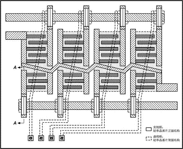
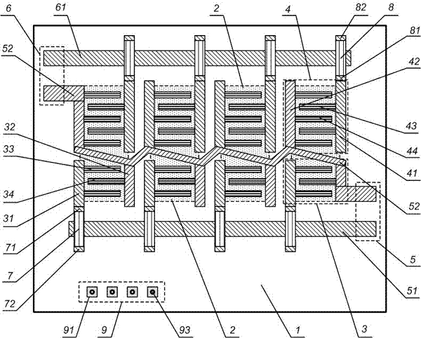
[0052] Such as figure 1 , 2 , 3 and 4 shows the structure of a monolithic integrated 4-unit surface acoustic wave filter component, including:

[0053] Silicon single crystal substrate 1, 4 zinc oxide piezoelectric thin film regions 2 fabricated on the front side of silicon single crystal substrate 1, 4 surface acoustic wave filter units respectively fabricated on the 4 zinc oxide piezoelectric thin film regions 2, 1 A surface acoustic wave filter unit includes an input IDT 3 and an output IDT 4;

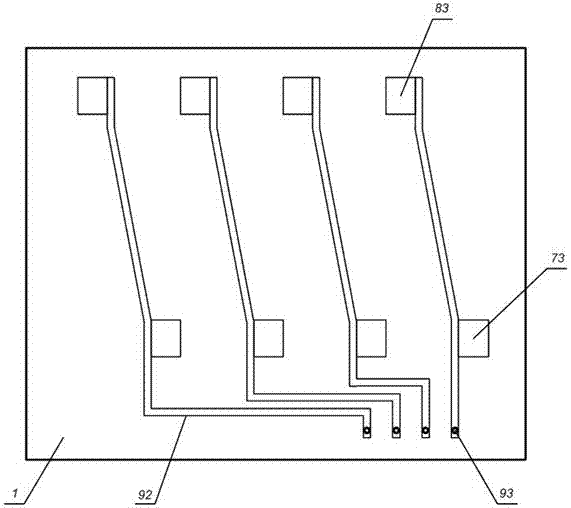
[0054] 4 input signal main electrodes 51 made outside the input IDT 3, output signal main electrodes 61 made outside the 4 output IDTs 4, the input IDT 3 and the output IDT The grounding total electrode 52 made between the 4 input ground terminal bus electrodes 32 and the 4 output ground terminal bus electrodes 42, the input signal general electrode 51...


PUM


Abstract

The invention relates to a single chip integrated acoustic surface wave filter component. The single chip integrated acoustic surface wave filter component comprises a silicon single crystal substrate, an acoustic surface wave filter unit arranged on the piezoelectric film region on the top of the silicon single crystal substrate, multiple groups of metal beams used for gating the filter unit and fixed electrodes thereof, an input signal total electrode, an output signal total electrode, a metal beam pull-down electrode and a pull-down signal input electrode of a control metal beam arranged at the back of the silicon single crystal substrate, and a pull-down signal input line. According to the invention, the interconnection structures are gated by the filter unit adopting the on-chip integration, and a micro mechanical switch with excellent dynamic and static characteristics is used as a gating switch element, therefore, the single chip integrated acoustic surface wave filter component has the advantages of compact structure, small radio frequency loss and good filter channel isolation.

Description

technical field [0001] The invention relates to an integrated surface acoustic wave device, in particular to a monolithic integrated surface acoustic wave filter component, belonging to the technical field of microelectronics. Background technique [0002] The surface acoustic wave filter converts the electrical signal into an acoustic signal by the input interdigital transducer fabricated on the piezoelectric substrate, the acoustic signal propagates along the surface of the substrate, and then converts the acoustic signal into an electrical signal by the output interdigital transducer , in the two conversions, the filtering function of the electrical signal is realized, that is, the electrical signal of a certain frequency band is allowed to pass and the electrical signal of other frequencies is suppressed. [0003] The surface acoustic wave filter component includes multiple surface acoustic wave filter units and their gating circuits, which can realize one or more inputs...

Claims


Application Information

Patent Timeline
IPC IPC(8): H03H9/02H03H9/64
CPCH03H9/02661H03H9/02818H03H9/6423
Inventor 赵成陈磊胡经国
Owner YANGZHOU UNIV
Why Eureka
Try Eureka