Micro light emitting diode and display panel

A technology of light-emitting diodes and display panels, applied in the direction of instruments, electrical components, circuits, etc., can solve the problems of mutual contact between electrodes, decrease in the manufacturing yield of micro light-emitting diode display panels, short circuits, etc., to avoid cracks, reduce short circuits and cracks chance, the effect of distributing joint pressure

Active Publication Date: 2019-01-15
PLAYNITRIDE
View PDF3 Cites 16 Cited by
  • Summary
  • Abstract
  • Description
  • Claims
  • Application Information

AI Technical Summary

Problems solved by technology

However, the electrodes subjected to pressure and heating will expand toward their two sides, and it is easy to make adjacent electrodes contact each other, resulting in a short circuit (Short Circuit), which reduces the manufacturing yield of the micro-LED display panel. decline
At the same time, it will also cause defective pixels in the micro-LED display panel, resulting in poor image quality of the display panel.

Method used


Image

  • Micro light emitting diode and display panel
  • Micro light emitting diode and display panel
  • Micro light emitting diode and display panel

Examples


Embodiment Construction

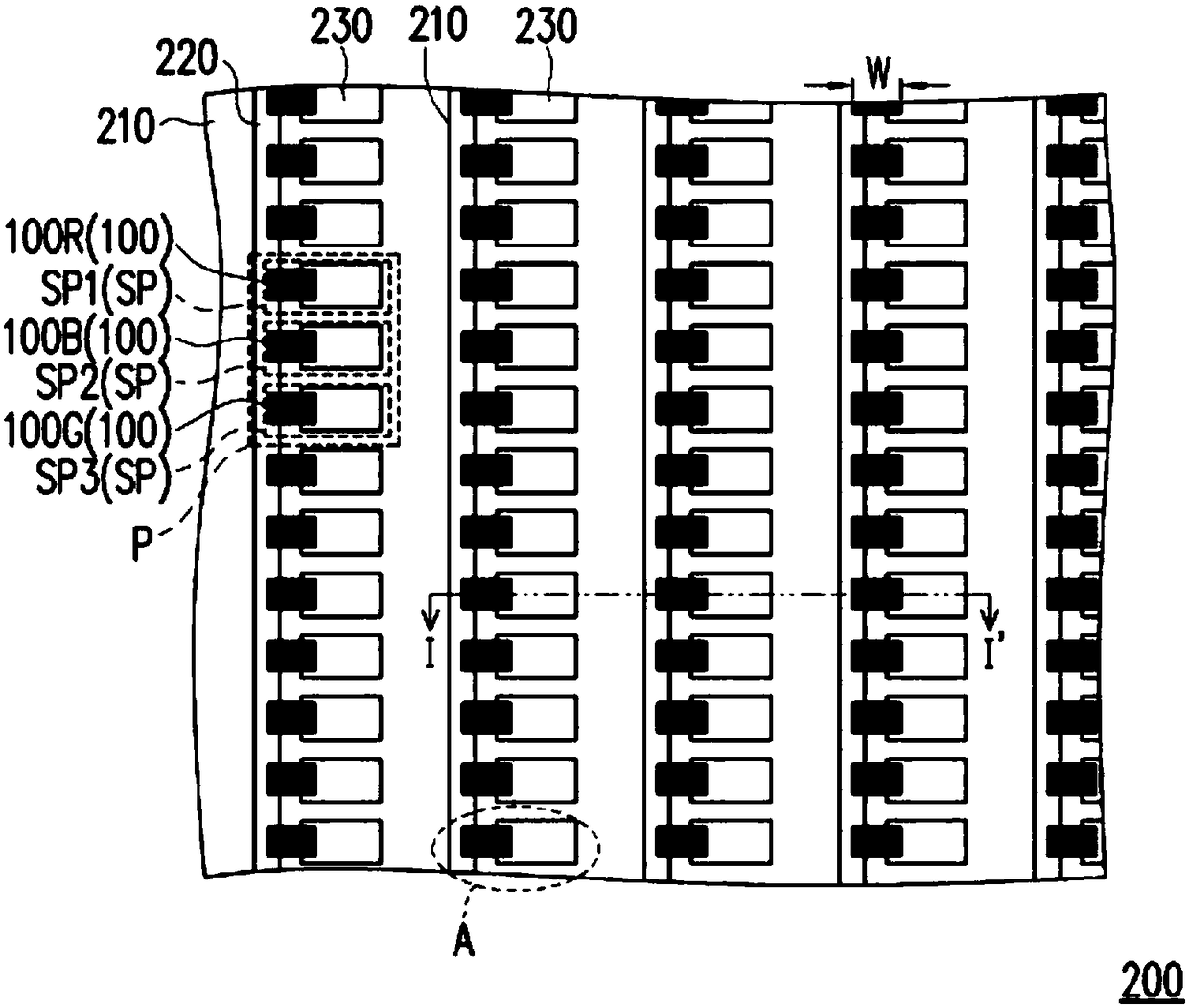
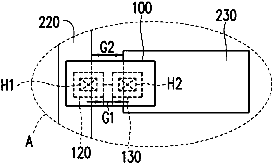
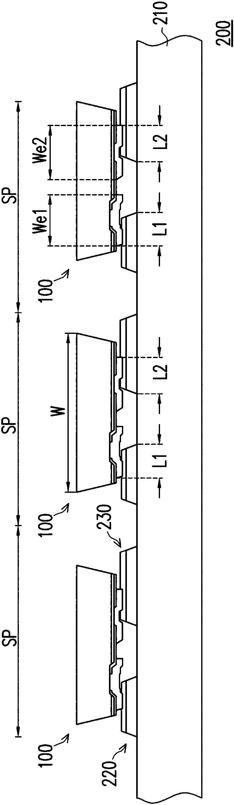
[0059] Please refer to Figure 1A , Figure 1B as well as Figure 2A , which is an embodiment of the display panel of the present invention. In this embodiment, the display panel 200 is embodied as a Micro Light Emitting Diode Display (Micro Light Emitting Diode Display). The display panel 200 includes a backplane 210 and a plurality of miniature light emitting diodes 100 . The backplane 210 has a plurality of sub-pixels SP, and one micro-LED 100 is located in one sub-pixel SP. Please refer to Figure 1A, in this embodiment, three sub-pixels SP1, SP2, SP3 form a display pixel P. A red micro LED 100R is arranged in the sub-pixel SP1, a blue micro LED 100B is arranged in the sub-pixel SP2, and a green micro-LED 100G is arranged in the sub-pixel SP3, but this is not the case in the present invention limit. The miniature light-emitting diodes 100 are electrically connected to the backplane 210 . In detail, in this embodiment, the display panel 200 controls the light-emitting...


PUM


Abstract

A miniature light emitting diode includes an epitaxial layer, an insulating layer, a first electrode, and a second electrode. The insulating layer is located on the surface of the epitaxial layer andhas a first consistent hole and a second through hole. The first electrode is electrically connected to the first type semiconductor layer of the epitaxial layer via the first uniform hole, and has aplurality of first electrode plateau portions. These first electrode platforms have different horizontal heights with respect to the epitaxial layer, respectively. The second electrode is electricallyconnected to the second type semiconductor layer of the epitaxial layer via the second through hole, and has a plurality of second electrode platforms. These second electrode platforms have differenthorizontal heights with respect to the epitaxial layer. In addition, a display panel is also proposed.

Description

technical field [0001] The present invention relates to a light emitting diode and a display panel, in particular to a micro light emitting diode (MicroLight Emitting Diode, μLED) and a display panel having the micro light emitting diode. Background technique [0002] Miniature light-emitting diodes have self-luminous display characteristics. Compared with the organic light emitting diode (Organic Light Emitting Diode, OLED) technology, which is also a self-luminous display, the micro light emitting diode not only has high efficiency, long lifespan, but also relatively stable materials that are not easily affected by the environment. Therefore, miniature light-emitting diodes are expected to surpass the organic light-emitting diode display technology and become the mainstream of future display technology. [0003] However, due to their small size, miniature light-emitting diodes also encounter many technical bottlenecks during bonding. For example, since the micro light em...

Claims


Application Information

Patent Timeline
Patent Type & Authority Applications(China)
IPC IPC(8): H01L33/02H01L33/38G09F9/33
CPCG09F9/33H01L33/02H01L33/382
Inventor 赖育弘罗玉云林子旸
Owner PLAYNITRIDE
Why Eureka
Try Eureka