Eureka AIR delivers breakthrough ideas for toughest innovation challenges, trusted by R&D personnel around the world.

TFT substrate

A substrate and substrate layer technology, applied in the direction of instruments, electrical components, circuits, etc., can solve the problems of PI liquid inflow, traces, uneven brightness of the display, etc., and achieve the effect of avoiding the problem of PImura

Inactive Publication Date: 2019-01-18
TCL CHINA STAR OPTOELECTRONICS TECH CO LTD
View PDF3 Cites 6 Cited by
  • Summary
  • Abstract
  • Description
  • Claims
  • Application Information

AI Technical Summary

Problems solved by technology

[0005] In this way, when the PI liquid is coated on the TFT substrate, due to the effect of the surface tension of the PI liquid, the PI liquid cannot flow into the via hole, which in turn causes the PI liquid to accumulate around the via hole, forming PI mura (refers to the uneven brightness of the display, causing various traces)
After the PI liquid is baked to form the alignment film, since the coating of the PI liquid is not uniform, there is a problem of accumulation around the via holes, which affects the uniform film thickness of the alignment film. characteristics, resulting in uneven brightness of the display

Method used


Image

  • TFT substrate
  • TFT substrate

Examples


Embodiment 1

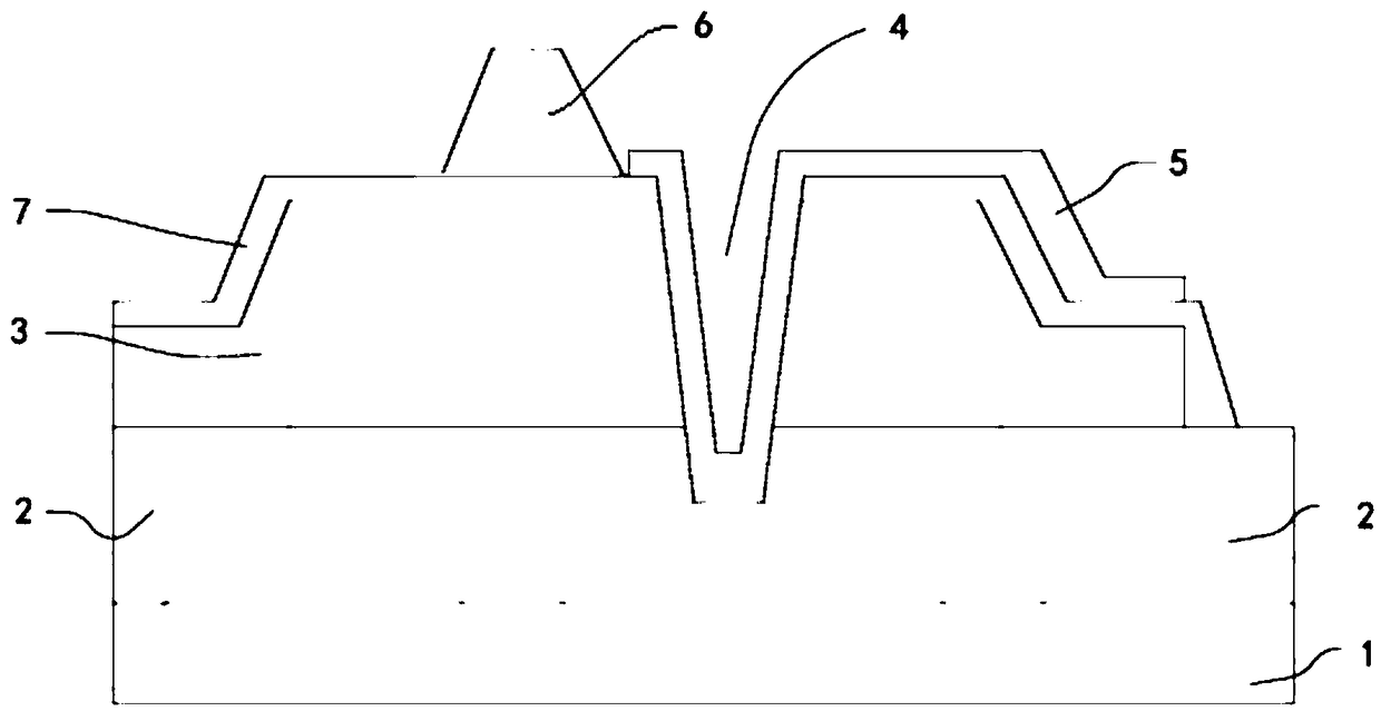
[0027] like figure 1 As shown, an embodiment of the present invention provides a TFT substrate, including a substrate layer 1, a thin film transistor 2, a color resistance layer 3, a via hole 4 and a pixel electrode 5, wherein the via hole 4 passes through the color resistance layer 3 so that the pixel The electrode 5 is connected to the thin film transistor 2 .

[0028] Wherein the color resistance layer 3 is also provided with a protrusion 6, which is arranged on one side of the via hole 4, and when the color resistance layer 3 is coated with PI liquid (polyimide liquid), the protrusion 6 can block the The surface tension of the PI liquid enables it to flow smoothly into and fill the via hole 4 .

[0029] In this embodiment, the protrusion 6 is made of a color-resist material and is formed by exposure. The color-resisting material involved includes one of the color-resisting materials such as R / G / B / Ps / BM, which can be specified according to needs and is not limited.

[00...

Embodiment 2

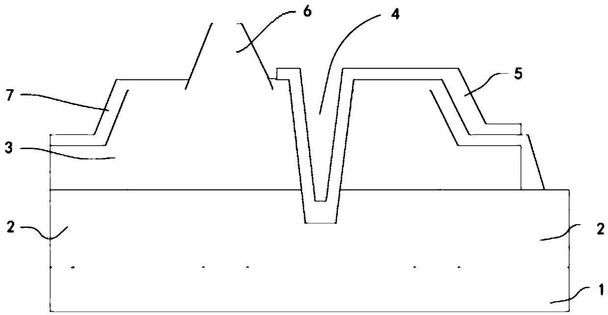
[0037] like figure 2 As shown, another embodiment of the present invention provides all the technical solutions including the TFT substrate of Embodiment 1, the difference is that the protrusion 6 and the color resist layer 3 are integrally formed. That is, a part of the color resist layer 3 protrudes upward to form a protrusion 6 . The protrusion 6 and the color-resist layer 3 are integrally formed, which can increase the stability between the protrusion 6 and the substrate and prevent it from falling off.

[0038] The beneficial effect of the present invention is: a kind of TFT substrate that the present invention relates to, it is by setting the protrusion 6 structure beside its via hole 4, to drain PI liquid to flow into the via hole 4, avoid PI liquid because of its own surface tension problem. The resulting accumulation around the via hole 4 effectively avoids the PI mura problem.

[0039] Further, the PI liquid will fill the via holes 4 after flowing into them, so th...


PUM


Abstract

The invention discloses a TFT substrate. The TFT substrate comprises a substrate layer, a thin-film transistor, a color resistance layer, a via hole and a pixel electrode; the via hole penetrates thecolor resistance layer so that the pixel electrode and the thin-film transistor are conducted; the color resistance layer is characterized in that a bulge is formed thereon, the bulge is arranged at one side of the via hole; when coating PI solution (polyimide solution) on the color resistance layer, the bulge can obstruct the surface tension of the PI solution, so that the PI solution can flatlyflow in and fill the via hole. The TFT substrate disclosed by the invention has the advantages that a bulge structure is arranged beside the via hole so as to guide the PI solution to flow in the viahole, the condition that the PI solution is stacked around the via hole due to the problem of the own surface tension, and then the PI mura problem is effectively avoided.

Description

technical field [0001] The invention relates to the field of plane display technology, in particular, a TFT substrate therein. Background technique [0002] Existing displays mainly include liquid crystal (Liquid Crystal Display, LCD) displays and OLED (Organic Light Emitting Diode) displays. [0003] The liquid crystal display generally includes a TFT panel. During its manufacturing process, PI (Polyimide, polyimide) liquid is coated on the substrate, and after baking, it becomes an alignment film, which is used to provide a pre-tilt angle for the liquid crystal molecules. , so that the rotation directions of the liquid crystal molecules are consistent. The film thickness uniformity of the alignment film directly affects the display effect of the TFT-LCD. [0004] With the development of technologies such as COA (Color filter On Array, the color photoresist layer is prepared on the array substrate), more via holes (Via holes) will be provided on the TFT substrate for diff...

Claims


Application Information

Patent Timeline
IPC IPC(8): G02F1/1362G02F1/1368G02F1/1337H01L27/12
CPCG02F1/133723G02F1/136227G02F1/1368G02F1/136222H01L27/1214
Inventor 朱清永程全
Owner TCL CHINA STAR OPTOELECTRONICS TECH CO LTD
Why Eureka
Eureka Blog
Learn More