Eureka AIR delivers breakthrough ideas for toughest innovation challenges, trusted by R&D personnel around the world.

Negative boosting circuit, semiconductor device and electronic device

A negative boost, boost capacitor technology, applied in instruments, static memory, read-only memory, etc., can solve the problems affecting the performance of P-type multiple programmable memory, improve the read operation performance and reduce the gap, Effects of small temperature and process variations

Active Publication Date: 2019-01-29
SEMICON MFG INT (SHANGHAI) CORP +1
View PDF4 Cites 3 Cited by
  • Summary
  • Abstract
  • Description
  • Claims
  • Application Information

AI Technical Summary

Problems solved by technology

The negative bias voltage is generally generated by a negative boost circuit, and the level of the bias voltage is affected by the operating voltage VCC, temperature and process variation (ie process angle), thus affecting the P-type multiple programmable ( MTP) memory performance

Method used


Image

  • Negative boosting circuit, semiconductor device and electronic device
  • Negative boosting circuit, semiconductor device and electronic device
  • Negative boosting circuit, semiconductor device and electronic device

Examples


Embodiment Construction

[0037] In the following description, numerous specific details are given in order to provide a more thorough understanding of the present invention. It will be apparent, however, to one skilled in the art that the present invention may be practiced without one or more of these details. In other examples, some technical features known in the art are not described in order to avoid confusion with the present invention.

[0038] It should be understood that the invention can be embodied in different forms and should not be construed as limited to the embodiments set forth herein. Rather, these embodiments are provided so that this disclosure will be thorough and complete, and will fully convey the scope of the invention to those skilled in the art. In the drawings, the size and relative sizes of layers and regions may be exaggerated for clarity, and like reference numerals designate like elements throughout.

[0039] It will be understood that when an element or layer is referr...


PUM


Abstract

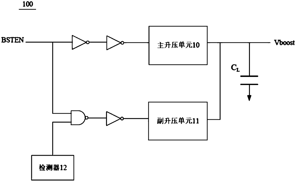
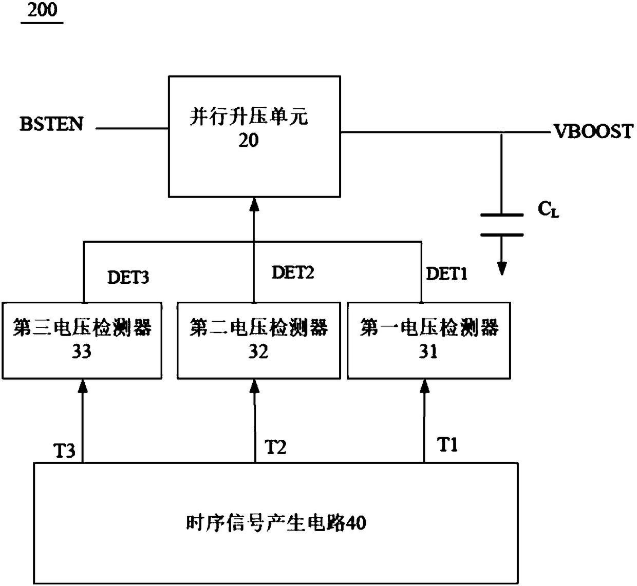
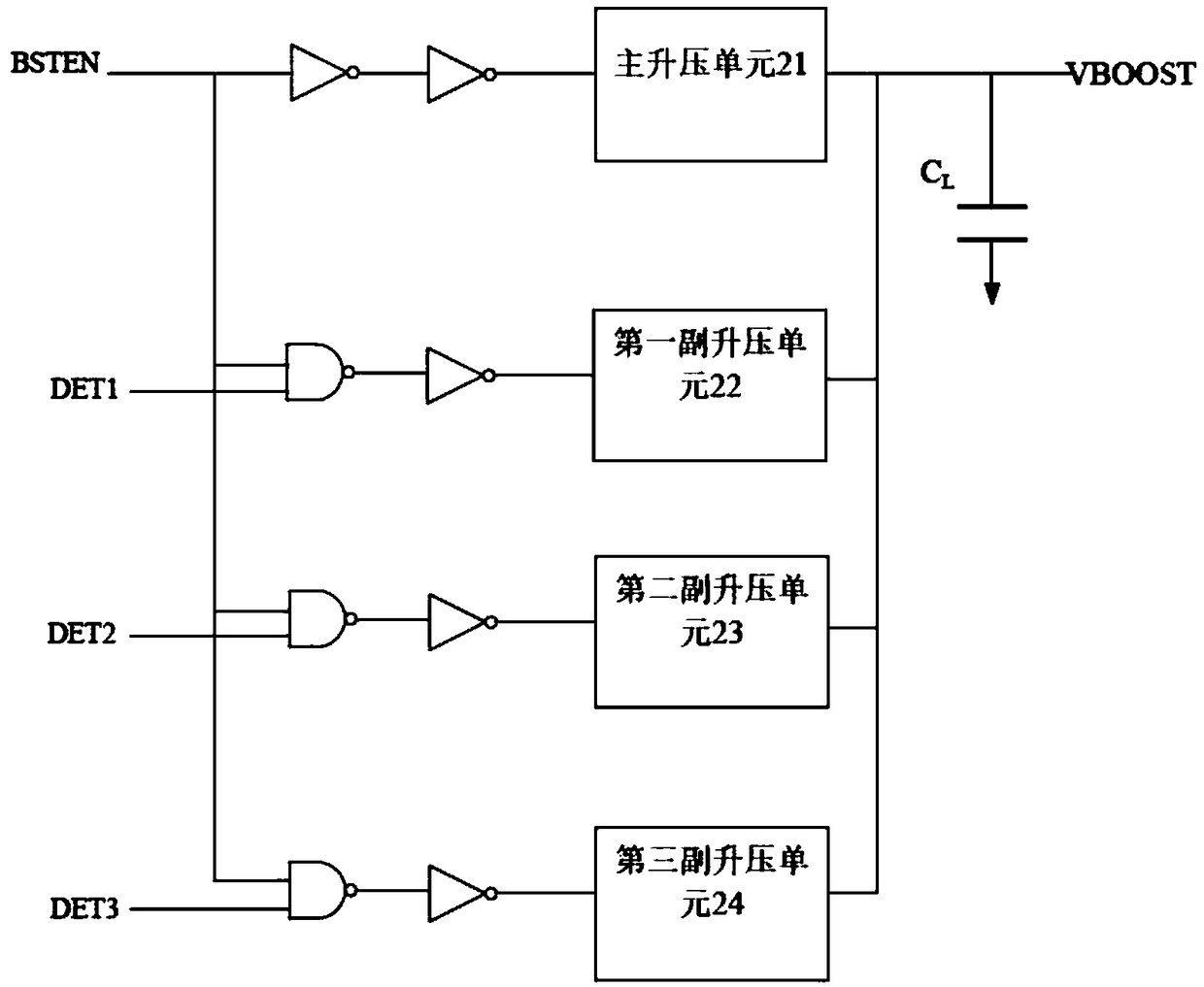
The invention provides a negative boosting circuit, a semiconductor device and an electronic device. The negative boost circuit includes a main boost unit configured to generate a basic bias signal; asub-boost unit configured to be connected in parallel with the main boost unit for generating an additional bias signal to form the negative bias together with the base bias signal; a voltage detector configured to generate a voltage detection signal acting on the sub-boosting unit based on a voltage at an output terminal of the negative boosting circuit, the voltage detection signal causing thesub-boosting unit to generate the additional bias signal, wherein the number of the sub-boosting units is 2 or more, and each of the sub-boosting units is provided with a voltage detector corresponding to the sub-boosting units. The negative boost circuit of the invention can reduce the influence of VCC, temperature and process on the negative bias voltage, and reduce the difference of the negative bias voltage of each working condition. The semiconductor device and the electronic device of the present invention have better read operation performance.

Description

technical field [0001] The invention relates to the technical field of semiconductors, in particular to a negative boost circuit, a semiconductor device and an electronic device. Background technique [0002] P-type multiple-time programmable (MTP) memory has multiple operations of programming, erasing and reading, and it requires a negative bias of -1.5*VCC during the reading operation. The negative bias voltage is generally generated by a negative boost circuit, and the level of the bias voltage is affected by the operating voltage VCC, temperature and process variation (ie process angle), thus affecting the P-type multiple programmable ( MTP) memory performance. [0003] Therefore, it is necessary to provide a negative boost circuit, a semiconductor device and an electronic device to at least partially solve the above problems. Contents of the invention [0004] A series of concepts in simplified form are introduced in the Summary of the Invention, which will be furth...

Claims


Application Information

Patent Timeline
IPC IPC(8): G11C5/14G11C16/30
CPCG11C5/147G11C16/30
Inventor 权彝振倪昊刘晓艳
Owner SEMICON MFG INT (SHANGHAI) CORP
Why Eureka
Eureka Blog
Learn More