Electron beam control device and method, electron beam imaging module and electron beam detection device

An electron beam imaging and control device technology, applied in the field of image processing, can solve the problems that cannot be used for fine inspection and cannot realize functional integration

Active Publication Date: 2019-02-01
DONGFANG JINGYUAN ELECTRON LTD
View PDF5 Cites 2 Cited by
  • Summary
  • Abstract
  • Description
  • Claims
  • Application Information

AI Technical Summary

Problems solved by technology

[0003] However, conventional methods for increasing the inspection speed of electron beam inspection equipment usually use large pixel sizes and large beam currents to achieve high-speed scanning of the inspected area, but this method cannot be

Method used


Image

  • Electron beam control device and method, electron beam imaging module and electron beam detection device
  • Electron beam control device and method, electron beam imaging module and electron beam detection device
  • Electron beam control device and method, electron beam imaging module and electron beam detection device

Examples


Embodiment Construction

[0032] The technical solutions of the present disclosure will be further explained in detail by means of embodiments in conjunction with the accompanying drawings. In the specification, the same or similar reference numerals and letters designate the same or similar components. The following description of the embodiments of the present disclosure with reference to the accompanying drawings is intended to explain the general inventive concept of the present disclosure, and should not be construed as a limitation of the present disclosure.

[0033] The accompanying drawings are used to illustrate the content of the present disclosure. The dimensions and shapes of the components in the drawings do not reflect the true proportions of the components of the electron beam control device, electron beam imaging module, and electron beam detection equipment.

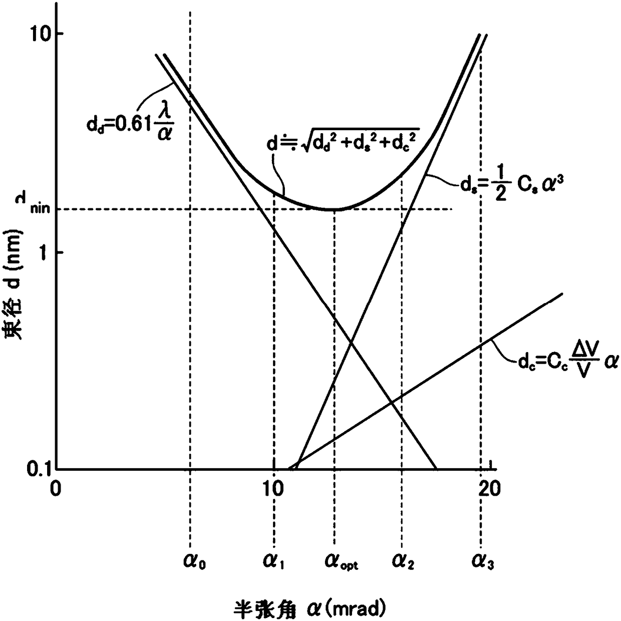
[0034] First, the working principle on which the present disclosure is based is explained.

[0035] figure 1 A schematic graph...


PUM


Abstract

The invention provides an electron beam control device for adjusting the size of an incident electron beam, a method, an electron beam imaging module and an electron beam detection device. The electron beam control device for adjusting the size of an incident electron beam comprises a diaphragm part; the diaphragm part is provided with multiple diaphragm openings arranged at intervals; the positions of the multiple diaphragm openings in the diaphragm part are determined to be corresponding to multiple different half angles of the incident electron beams and different sizes of the electron beams; and the size of each diaphragm opening is determined to be enough to enable the electron beam with the corresponding size to pass through, and thus, the size of the incident electron beam can be moved to the selected diaphragm opening in the multiple diaphragm openings to be adjusted through the electron beam.

Description

technical field [0001] The present disclosure relates to the field of image processing, and in particular to an electron beam control device and method for image acquisition, an electron beam imaging module, and an electron beam detection device. Background technique [0002] In recent years, the use of electron beam technology in vacuum to detect and measure the critical dimensions of the fine patterns on semiconductor silicon wafers or reticles has gradually been widely used, such as including but not limited to: Dimensional measuring equipment such as scanning electron microscope (CD-SEM), review equipment that performs re-inspection in a precise observation method for the defects detected by the electron beam inspection device, such as review scanning electron microscope (Review SEM), uses a computer to measure the occurrence rate of defects. Graphical defect detection equipment for predicting the region, etc. The above-mentioned equipment not only needs to realize the ...

Claims


Application Information

Patent Timeline
IPC IPC(8): H01J37/28H01J37/09
CPCG01N23/04H01J37/09H01J37/28
Inventor 滝川忠宏
Owner DONGFANG JINGYUAN ELECTRON LTD
Why Eureka
Try Eureka