Aging device and aging method for laser device chip

An aging device and laser technology, applied in the direction of measuring devices, measuring device shells, electrical measuring instrument components, etc., can solve problems such as difficult direct clamping, time-consuming reliability, easy damage and dirt, and reduce damage to chips Possibility, convenient and fast power supply, simple operation effect

Inactive Publication Date: 2019-02-12
WUHAN TELECOMM DEVICES
View PDF15 Cites 12 Cited by
  • Summary
  • Abstract
  • Description
  • Claims
  • Application Information

AI Technical Summary

Problems solved by technology

However, the size of the laser chip is usually very small, the length, width and height are less than 1 mm, generally only a few tenths of a mm, it is not easy to be directly clamped, and it is easy to be damaged and dirty, and it is also difficult to power the laser chip during the aging process.
Therefore, in the process of manufacturing TOSA, the aging process of the laser chip is very difficult, time-consuming and has low reliability, which is not conducive to the mass production of TOSA. This is a difficult problem in the entire optical communication device manufacturing industry.

Method used


Image

  • Aging device and aging method for laser device chip
  • Aging device and aging method for laser device chip
  • Aging device and aging method for laser device chip

Examples


Embodiment 1

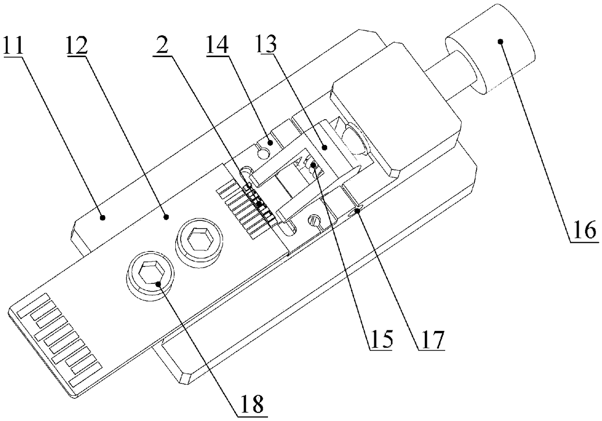
[0040] An embodiment of the present invention provides an aging device for a laser chip, such as Figure 1-Figure 3 As shown, it includes a clamp 1 and a chip component 2 , and the clamp 1 is used to clamp the chip component 2 . Wherein, considering that the size of the laser chip is very small, it is not easy to clamp, and direct clamping is easy to cause damage, the method of clamping the chip assembly is adopted in the present invention, and the chip assembly 2 includes a laser chip 21 and a chip carrier, and the laser chip 21 fixed on the surface of the chip carrier, the chip carrier is used to be clamped, since the size of the chip carrier is much larger than the laser chip, it is easier to clamp and will not cause damage to the laser chip;

[0041]The clamp 1 includes a base 11, a PCB connecting plate 12 and a pressing block 13, the PCB connecting plate 12 is fixedly installed on the surface of the base 1, and the pressing block 13 is movably installed on the surface of ...

Embodiment 2

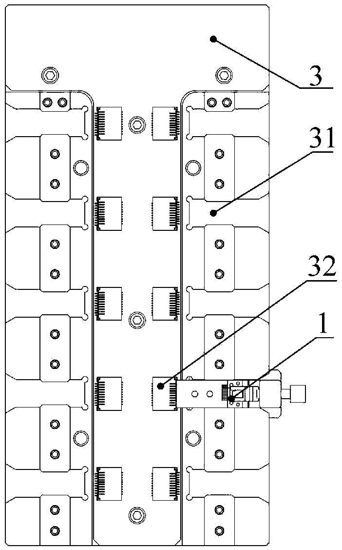
[0054]On the basis of the above-mentioned embodiment 1, the embodiment of the present invention also provides a laser chip aging method, which is completed by using the aging device in embodiment 1. Refer to Figure 10 , the aging method specifically includes the following steps:

[0055] Step 201, assemble the clamp 1, adjust the screw push rod 16, so that the first end of the pressing block 13 is in a tilted state.

[0056] according to figure 1 As shown, with reference to the structure introduction in Embodiment 1, the PCB connection plate 12, the positioning plate 14, the pressure block 13, the torsion spring 15 and the screw push rod 16 are respectively installed on the base Seat 11 surface, and by rotating the screw push rod 16, the pressure block 13 is as follows Figure 6 In the state shown, the left end of the pressure block 13 is in a tilted state under the tension of the torsion spring 15, so as to facilitate the placement of the chip assembly 2.

[0057] Step 20...


PUM


Abstract

The invention relates to the field of optical communication device manufacturing, and provides an aging device and an aging method for a laser device chip. The device comprises a clamp and a chip assembly, wherein the clamp is used for clamping the chip assembly, the chip assembly comprises the laser device chip and a chip carrier, and the laser device chip is fixed to the surface of the chip carrier; the clamp comprises a substrate and a PCB connecting plate, a positioning plate and a pressing block which are installed on the substrate in sequence, the positioning plate is used for placing and positioning the chip assembly, and the PCB connecting plate is used for the connection of the laser device chip and a power supply circuit; the pressing block is movably installed on the surface ofthe substrate, one end of the pressing block is positioned above the positioning plate, and the chip assembly can be compressed or loosened by rotating the pressing block. The laser device chip is fixedly pasted onto the chip carrier, the chip carrier can be clamped by the clamp directly conveniently, quickly, stably, reliably and accurately during aging, chip clamping is realized, the chip damageis reduced, and the clamp is simple in operation and low in cost and can be used repeatedly, so that the problem of chip aging is solved.

Description

【Technical field】 [0001] The invention relates to the field of manufacturing optical communication devices, in particular to an aging device and aging method for a laser chip. 【Background technique】 [0002] In the field of optical communication design and manufacturing, for active optical devices such as Transmitter Optical Subassembly (TOSA), in the manufacturing process, the aging process of the laser chip is an essential step. , which is of great significance to ensure the performance of the device, the stability of communication data and signal transmission, and the reliability of the device. [0003] According to industry rules, when chip manufacturers sell chips to device manufacturers, they usually do not implement the aging process on the chips, which requires device manufacturers to implement the aging process on the laser chips they purchase. However, the size of the laser chip is usually very small, the length, width and height are less than 1 mm, generally only...

Claims


Application Information

Patent Timeline
Patent Type & Authority Applications(China)
IPC IPC(8): G01R1/04G01R31/00
CPCG01R1/0408G01R1/0425G01R31/00
Inventor 梅晓鹤胡强薛振峰周芸全本庆
Owner WUHAN TELECOMM DEVICES
Why Eureka
Try Eureka