Display substrate, manufacturing method thereof, and display device
A technology for display substrates and manufacturing methods, which is applied in semiconductor/solid-state device manufacturing, electrical components, electric solid-state devices, etc., and can solve problems such as poor static electricity and broken wires of display substrates
- Summary
- Abstract
- Description
- Claims
- Application Information
AI Technical Summary
Problems solved by technology
Method used
Image

Examples
Embodiment 1
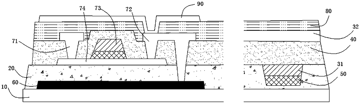
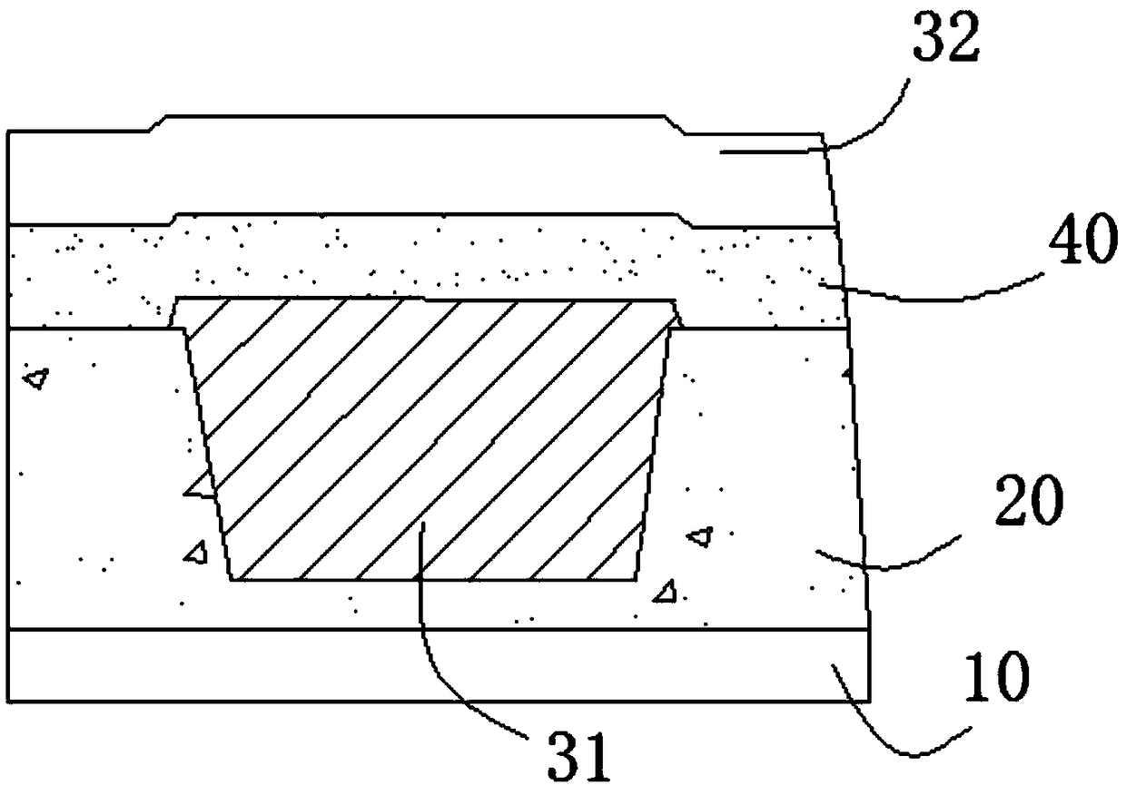
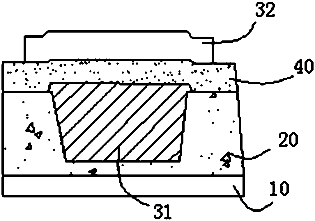
[0036] This embodiment provides a display substrate, including a base 10, a first insulating layer 20 disposed on the base 10, a first signal line 31 disposed on the side of the first insulating layer 20 away from the base 10, and a cover covering the first signal line 31. The second insulating layer 40, the second signal line 32 disposed on the side of the second insulating layer 40 away from the substrate 10, the first signal line 31 and the second signal line 32 have an overlapping area.
[0037] For example figure 1 with figure 2 As shown, the second insulating layer 40 separates the first signal line 31 and the second signal line 32 , and the two have an overlapping area.
[0038] A groove is provided on the first insulating layer 20 , and the first signal line 31 is disposed in the groove at least at the overlapping area.
[0039] In one embodiment, at least part of side surfaces of the first signal line 31 located in the groove are in contact with the wall of the gro...
Embodiment 2
[0063] This embodiment provides a method for manufacturing a display substrate. The display substrate is the display substrate provided in Embodiment 1. The manufacturing method includes:
[0064] forming a first insulating layer 20 on the substrate 10 through a patterning process, and forming grooves in the first insulating layer 20;
[0065] forming a first signal line 31 on the first insulating layer 20 through a patterning process;
[0066] forming a second insulating layer 40 on the first signal line 31;
[0067] The second signal line 32 is formed on the second insulating layer 40 through a patterning process.
[0068] That is, the first insulating layer 20 , the first signal line 31 , the second insulating layer 40 , and the second signal line 32 in Embodiment 1 are sequentially formed on the substrate 10 .
[0069] Optionally, when the first insulating layer 20 is formed using a silicone glass solution, forming the first insulating layer 20 on the substrate 10 throug...
Embodiment 3
[0095] This embodiment provides a display device, including the display substrate provided in Embodiment 1 of the present invention.
[0096] Specifically, the display device can be any product with a display function such as a liquid crystal display panel, an organic light-emitting diode (OLED) display panel, an electronic paper, a mobile phone, a tablet computer, a television set, a monitor, a notebook computer, a digital photo frame, a navigator, or the like. part.
PUM
 Abstract
Description
Claims
Application Information
 - R&D
- Intellectual Property
- Life Sciences
- Materials
- Tech Scout
- Unparalleled Data Quality
- Higher Quality Content
- 60% Fewer Hallucinations
Browse by: Latest US Patents, China's latest patents, Technical Efficacy Thesaurus, Application Domain, Technology Topic, Popular Technical Reports.
© 2025 PatSnap. All rights reserved.Legal|Privacy policy|Modern Slavery Act Transparency Statement|Sitemap|About US| Contact US: help@patsnap.com