LED flip chip packaging technology-based LED screen packaging process and LED screen

A flip-chip and LED screen technology, which is applied in the direction of identification devices, instruments, electrical components, etc., can solve the problems of poor heat dissipation, complicated LED display packaging process, and inability to make small pitches, so as to improve pixels and save soldering. Line link, solve the effect of internal virtual welding and disconnection

Pending Publication Date: 2021-12-10
江西兆驰晶显有限公司
View PDF0 Cites 0 Cited by
  • Summary
  • Abstract
  • Description
  • Claims
  • Application Information

AI Technical Summary

Problems solved by technology

[0004] In view of the above-mentioned shortcomings and deficiencies of the prior art, the present invention provides an LED screen packaging process and LED screen based on LED flip-chip packaging technology, which solves the problems of complicated LED display packaging process, inability to make small spacing and poor heat dissipation. technical issues

Method used


Image

  • LED flip chip packaging technology-based LED screen packaging process and LED screen
  • LED flip chip packaging technology-based LED screen packaging process and LED screen
  • LED flip chip packaging technology-based LED screen packaging process and LED screen

Examples


Embodiment Construction

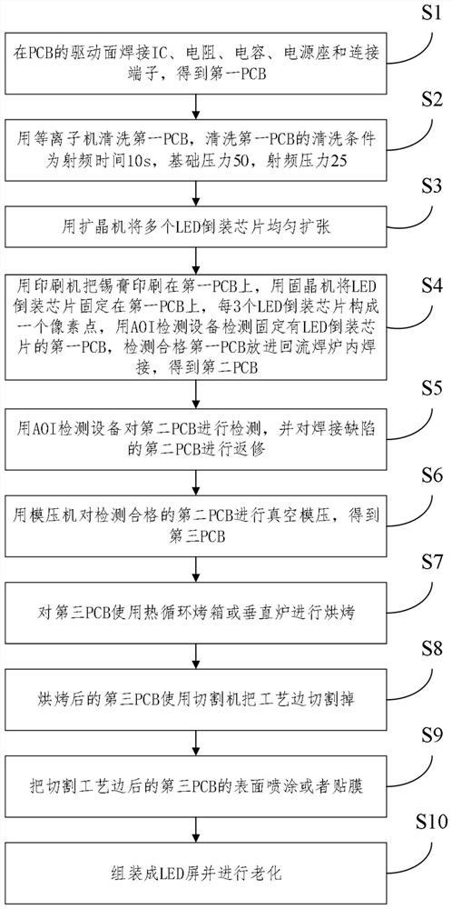
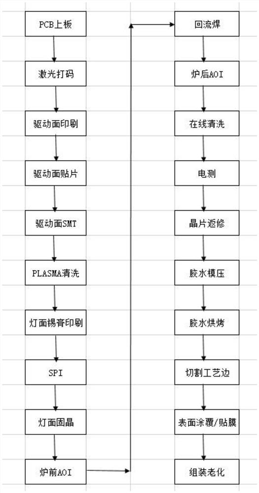
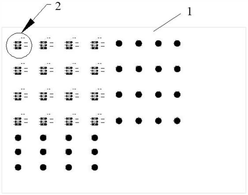
[0041] In order to better explain the present invention and facilitate understanding, the present invention will be described in detail below through specific embodiments in conjunction with the accompanying drawings. Among them, the orientation nouns such as "up" and "down" mentioned in this article are preceded by figure 1 orientation as a reference.

[0042] In order to better understand the above technical solutions, exemplary embodiments of the present invention will be described in more detail below with reference to the accompanying drawings. Although exemplary embodiments of the present invention are shown in the drawings, it should be understood that the invention may be embodied in various forms and should not be limited to the embodiments set forth herein. Rather, these embodiments are provided so that the present invention can be more clearly and thoroughly understood, and the scope of the present invention can be fully conveyed to those skilled in the art.

[00...


PUM


Abstract

The invention relates to an LED flip chip packaging technology-based LED screen packaging technology and an LED screen, and the packaging technology comprises the steps: welding an IC, a resistor, a capacitor, a power supply seat and a connection terminal on a PCB, and obtaining a first PCB; cleaning the first PCB, and uniformly expanding the plurality of LED flip chips by using a wafer expander; printing solder paste on the first PCB, fixing LED flip chips on the first PCB through a die bonder, enabling every three LED chips to form a pixel point, detecting the pixel point through AOI detection equipment, and putting qualified LED chips into a reflow soldering furnace to be welded into a second PCB; using the AOI detection equipment for detecting the second PCB, using a molding press to carry out out vacuum molding on the qualified second PCB to obtain a third PCB, after baking molding is carried out, according to the needed specification and size, cutting off unnecessary process edges, and carrying out coating or film pasting is carried out on the lamp face of the module. The surface is made to be black, the contrast ratio of the product is improved, and the color uniformity and consistency are improved, and the display effect is better; and each pixel point only needs six metal bonding points, so that a wire bonding link is omitted.

Description

technical field [0001] The invention relates to the technical field of LED display packaging, in particular to an LED screen packaging process based on LED flip-chip packaging technology and an LED screen. Background technique [0002] With the gradual maturity of LED (Light-emitting Diode) display technology, people have higher and higher requirements for the clarity of LED display screens, making high-definition LED display screens popular on a large scale. At present, the distance between adjacent pixels on most LED displays is 4mm, 3mm or 2.5mm, and mass production has begun. However, with the rapid development of LED display technology, people have put forward higher requirements for the pixels of LED displays. , and the LED display screens on the market can no longer meet the above requirements, and it is difficult to produce LED display screens with higher pixels by conventional packaging methods. The existing LED packaging methods include the following: the first is...

Claims


Application Information

Patent Timeline
Patent Type & Authority Applications(China)
IPC IPC(8): H01L21/67H01L27/15G09F9/33
CPCH01L21/67144H01L21/67121H01L27/156G09F9/33
Inventor 李铁军熊周成刘君宏
Owner 江西兆驰晶显有限公司
Why Eureka
Try Eureka