Tri-level carrier modulation method
A carrier modulation and three-level technology, applied to electrical components, output power conversion devices, AC power input conversion to DC power output, etc., to achieve the effect of simple and clear modulation method, strong reliability and easy realization
- Summary
- Abstract
- Description
- Claims
- Application Information
AI Technical Summary
Problems solved by technology
Method used
Image

Examples
Embodiment Construction
[0021] Embodiments of the present invention will be further described in detail below in conjunction with the accompanying drawings.
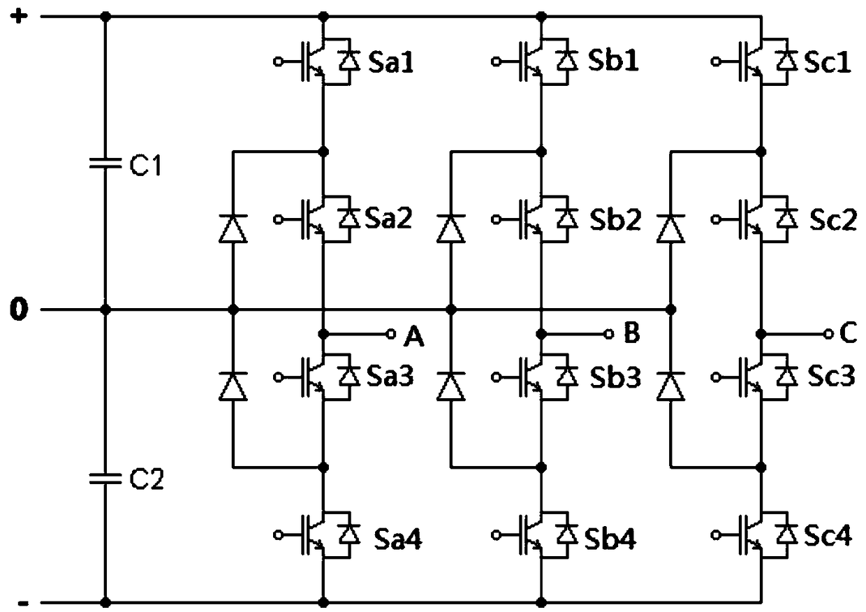
[0022] by figure 1 The typical three-level NPC frequency converter topology circuit is shown to illustrate the present invention; in the figure, C1 and C2 are DC capacitors, and Sa1~Sa4, Sb1~Sb4 and Sc1~Sc4 are the three phases of frequency converter A, B and C respectively Power switching devices and their anti-parallel diodes.
[0023] The three-level carrier modulation method of the present invention includes two modulation modes:
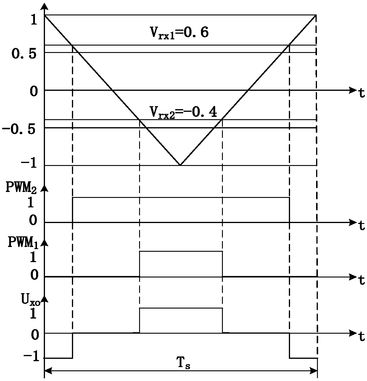
[0024] Mode 1: During one switching cycle, when the degree of modulation is less than V m , or the degree of modulation is greater than V m But the modulation wave V in the current carrier period rx The amplitude is less than Vm, that is, the modulation wave V rx When it is between [-Vm, Vm], mode 1 modulation is adopted.
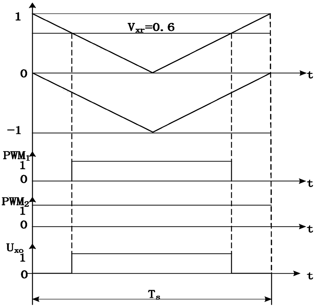
[0025] Mode 2: During one switching cycle, when the modulation degree is greater tha...
PUM
 Abstract
Description
Claims
Application Information
 - R&D
- Intellectual Property
- Life Sciences
- Materials
- Tech Scout
- Unparalleled Data Quality
- Higher Quality Content
- 60% Fewer Hallucinations
Browse by: Latest US Patents, China's latest patents, Technical Efficacy Thesaurus, Application Domain, Technology Topic, Popular Technical Reports.
© 2025 PatSnap. All rights reserved.Legal|Privacy policy|Modern Slavery Act Transparency Statement|Sitemap|About US| Contact US: help@patsnap.com