Modular CMOS imaging system

An imaging system and a modular technology, applied in parts of TV systems, image communication, and color TV parts, etc., can solve the problems of heavy design workload, long processing cycle, and high cost, so as to save construction time and reduce labor costs. The effect of low power consumption and good signal-to-noise ratio

Inactive Publication Date: 2019-02-19
CHANGCHUN INST OF OPTICS FINE MECHANICS & PHYSICS CHINESE ACAD OF SCI
View PDF6 Cites 3 Cited by
  • Summary
  • Abstract
  • Description
  • Claims
  • Application Information

AI Technical Summary

Problems solved by technology

[0003] In order to solve the imaging system of the existing CMOS image sensor, the present invention has the problems of large design workload, long processing cycle and high cost, and provides a modular CMOS imaging system

Method used


Image

  • Modular CMOS imaging system
  • Modular CMOS imaging system
  • Modular CMOS imaging system

Examples


specific Embodiment approach 1

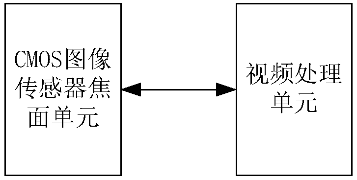
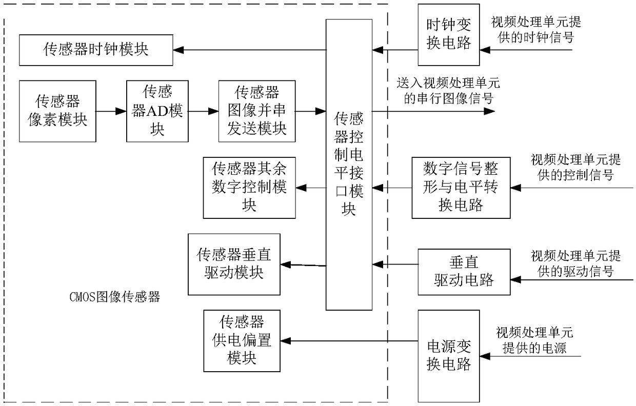
[0022] Specific implementation mode one, combination Figure 1 to Figure 6 Explaining this embodiment, the modular CMOS imaging system mainly includes two parts, the CMOS image sensor focal plane unit and the video processing unit, both of which can be composed of one or more circuit boards. The focal plane unit of the CMOS image sensor and the video processing unit are connected by connectors. For different CMOS image sensor applications, only the focal plane unit of the CMOS image sensor needs to be replaced, while the video processing unit remains unchanged.

[0023] There are many types of CMOS image sensors, including area arrays and linear arrays; linear arrays are divided into multi-spectral and single-spectrum, and can also be divided into TDI working mode devices and non-TDI working mode devices. The CMOS image sensor contains all or part of the sensor clock module, sensor pixel module, sensor AD module, sensor image parallel and serial transmission module, sensor vertica...


PUM


Abstract

The invention relates to a modular CMOS imaging system, which aims to solve such problems as a large designing workload, a long processing cycle and high cost of the conventional imaging system of CMOS image sensors. The modular CMOS imaging system comprises a CMOS image sensor focal plane unit and a video processing unit, wherein the CMOS image sensor focal plane unit and the video processing unit are connected through a connector; and the CMOS image sensor focal plane unit comprises a CMOS image sensor, a clock switching circuit, a digital signal shaping and level converting circuit, a vertical driving circuit, and a power switching circuit. When the imaging system is applied to different CMOS sensors, only the corresponding CMOS image sensor focal plane units need to be replaced, and replacement of the video processing unit is avoided, so that the work cycle is greatly shortened, the cost is greatly lowered, and the designing risk is reduced; and power supplies of the CMOS image sensors are classified into multiple types, and two or more adjustable power supplies are used to respectively supply power, so that the power efficiency is improved, the total power consumption is reduced, and thermal deformation of an optical-mechanical structure caused by heating of a focal plane sensor is alleviated.

Description

Technical field [0001] The present invention relates to a modular CMOS imaging system, in particular to a universal modular imaging system compatible with multiple CMOS image sensors such as area array, single-spectrum linear array, multi-spectral linear array, TDICMOS and the like. Background technique [0002] There are many types of CMOS image sensors, including area arrays and linear arrays; linear arrays are divided into multi-spectral and single-spectrum, and can also be divided into TDI working mode devices and non-TDI working mode devices. Different CMOS image sensors require different types and quantities of operating voltages, and require different input clock types, control signals and output data methods. If a specific imaging system is designed for each CMOS image sensor, there will be a design workload Large, long processing cycle and high cost. Summary of the invention [0003] The present invention provides a modular CMOS imaging system in order to solve the probl...

Claims


Application Information

Patent Timeline
IPC IPC(8): H04N5/374H04N5/376
CPCH04N25/745H04N25/76
Inventor 余达刘金国梅贵张宇王钢裴君妍朱立禄
Owner CHANGCHUN INST OF OPTICS FINE MECHANICS & PHYSICS CHINESE ACAD OF SCI
Why Eureka
Try Eureka