A feeding and discharging machine for semiconductor packaging

A semiconductor and material machine technology, used in semiconductor/solid-state device manufacturing, conveyor objects, transportation and packaging, etc., can solve the problems of cumbersome operating procedures, low packaging efficiency, and waste of labor, reducing manual participation and improving. High packaging efficiency and high packaging accuracy

Active Publication Date: 2019-02-26
东莞胜镁特工业科技有限公司
View PDF3 Cites 2 Cited by
  • Summary
  • Abstract
  • Description
  • Claims
  • Application Information

AI Technical Summary

Problems solved by technology

[0003] In order to solve the existing problems of cumbersome operation process, high manpower waste and low packaging efficiency caused by manual loading and unloading operations, the present invention proposes a semiconductor packaging loading and unloading machine

Method used


Image

  • A feeding and discharging machine for semiconductor packaging
  • A feeding and discharging machine for semiconductor packaging
  • A feeding and discharging machine for semiconductor packaging

Examples


Embodiment Construction

[0022] In order to better understand the present invention, the technical solutions of the present invention will be clearly and completely described below through examples. Apparently, the described examples are only some, not all, examples of the present invention. Based on the embodiments of the present invention, all other embodiments obtained by persons of ordinary skill in the art without making creative efforts belong to the protection scope of the present invention.

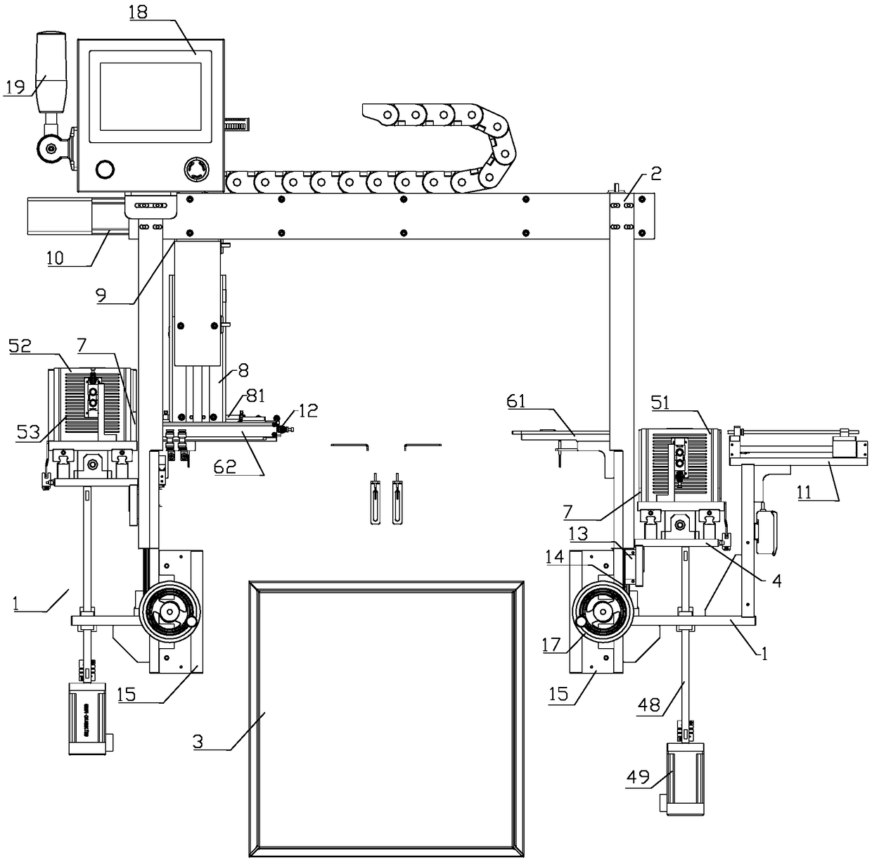
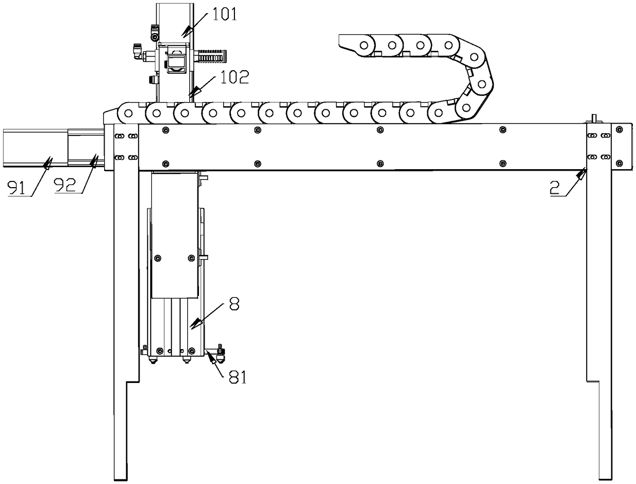
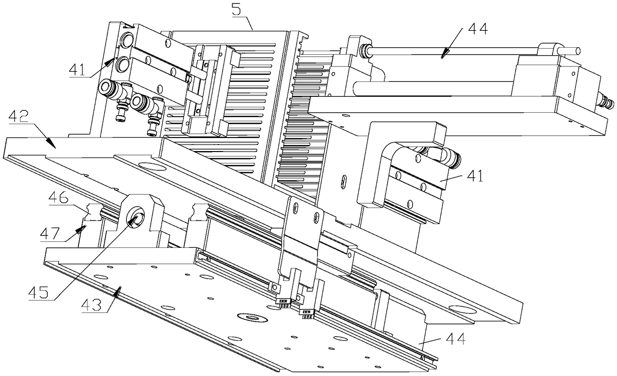
[0023] Such as Figure 1 to Figure 4 As shown, a semiconductor package loading and unloading machine includes a material table 1, a support 2 and an electric control box 3, two material tables 1 are provided, and the two material tables 1 are connected to the left and right sides of the support 2, and the material table 1 is respectively Movable seat 4 is set, and feed box 5 is installed on movable seat 4, and feed box 5 is divided into feed box 51 and discharge box 52, and semiconductor is contained in f...


PUM


Abstract

A feeding and discharging machine for semiconductor packaging comprises material tables, a support and an electric control box. A movable seat is arranged on each material table; material boxes are mounted on the movable seats; the material boxes include a feeding box and a discharging box; semiconductors are placed in the feeding box; the support is positioned between the feeding box and the discharging box; tracks are installed on the support; feeding ports are arranged between the tracks and the material boxes and the tracks include a feeding track and a discharging track; the feeding box is located between the feeding track and a feeding cylinder; the feeding cylinder pushes the semiconductors in the feeding box into the feeding track; a movable grab block is installed on the support and a vacuum sucker is arranged under the movable grab block; the movable grab block grabs the semiconductors via the vacuum sucker; the discharging track is located between a discharging cylinder andthe discharging box; the discharging cylinder pushes the packaged semiconductors in the discharging track to the discharging box. The machine realizes automatic feeding and discharging of semiconductors, simplifies the operation processes, reduces the manual participation of workers, and improves the packaging efficiency, and has good safety and high packaging accuracy.

Description

technical field [0001] The invention belongs to the technical field of semiconductor packaging, in particular to a semiconductor packaging loading and unloading machine. Background technique [0002] With the rapid development of the semiconductor packaging industry, the demand for semiconductors continues to increase. Traditional semiconductor packaging equipment mainly relies on manual loading, positioning, and unloading. Due to manual loading and unloading operations, the operation process of the staff is cumbersome, the waste of manpower is high, and one person can only operate 2 to 3 pieces of equipment, which ultimately makes the entire The packaging efficiency of the device cannot be improved. Contents of the invention [0003] In order to solve the existing problems of cumbersome operation process, high manpower waste and low packaging efficiency caused by manual loading and unloading operations, the present invention proposes a semiconductor packaging loading and...

Claims


Application Information

Patent Timeline
Patent Type & Authority Applications(China)
IPC IPC(8): H01L21/677
CPCH01L21/67706H01L21/67736
Inventor 王强笪宏兵
Owner 东莞胜镁特工业科技有限公司
Why Eureka
Try Eureka