A kind of organic electroluminescent device and its preparation method and display device

An electroluminescence device and electroluminescence technology, which are applied in the fields of electric solid state devices, semiconductor/solid state device manufacturing, electrical components, etc., and can solve the problems of high triplet exciton concentration, decreased device stability, and triplet exciton annihilation. , to achieve the effect of inhibiting molecular bond breakage, improving stability and reducing long life.

Active Publication Date: 2020-12-15
KUNSHAN GO VISIONOX OPTO ELECTRONICS CO LTD +1
View PDF5 Cites 1 Cited by
  • Summary
  • Abstract
  • Description
  • Claims
  • Application Information

AI Technical Summary

Problems solved by technology

Higher triplet excitons often lead to decreased device stability and reduced device lifetime
In addition, the concentration of triplet excitons in TADF materials is too high, and the annihilation phenomenon between triplet excitons is serious, resulting in serious efficiency roll-off.

Method used


Image

  • A kind of organic electroluminescent device and its preparation method and display device
  • A kind of organic electroluminescent device and its preparation method and display device
  • A kind of organic electroluminescent device and its preparation method and display device

Examples


preparation example Construction

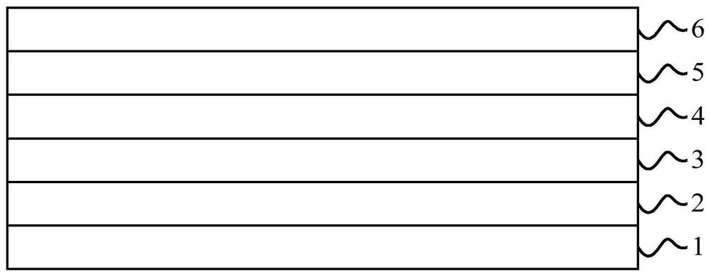
[0072] The present invention also provides a preparation method of the organic electroluminescent device, to figure 1 As an example, it includes sequentially depositing an anode 2 , a hole transport region 3 , a light emitting layer 4 , an electron transport region 5 , and a cathode 6 on a substrate 1 , and then packaging. Wherein, when preparing the light emitting layer 4, the light emitting layer 4 is formed by co-evaporating the triplet-triplet annihilation material source and the thermally activated delayed fluorescent material source.

[0073] Specifically, the preparation method of the organic electroluminescent device of the present invention comprises the following steps:

[0074] 1. Ultrasonically treat the glass plate coated with the anode material in a commercial cleaning agent, rinse in deionized water, ultrasonically degrease in acetone: ethanol mixed solvent, bake in a clean environment until the water is completely removed, and use ultraviolet light Light and o...

Embodiment 1-21

[0083] Embodiment 1-21 provides a kind of organic electroluminescent device respectively, and its device structure comprises ITO anode, hole injection layer (HIL), hole transport layer (HTL), light-emitting layer (EML), electron transport layer (ETL) successively. ), the electron injection layer (EIL) and the cathode.

[0084] Wherein, the material of the hole injection layer is HI-2, and the general total thickness is 5-30nm, which is 10nm in this embodiment. The material of the hole transport layer is HT-28, and the total thickness is generally 5-50 nm, which is 50 nm in this embodiment. The host material of the light-emitting layer is TTA material, the dye is TADF material, the doping concentration of the dye is 0.1-40wt%, and the thickness of the light-emitting layer is generally 1-60nm, which is 30nm in this embodiment. The material of the electron transport layer is ET-53, and the thickness is generally 5-30nm, which is 30nm in this embodiment. LiF (0.5nm) and metal al...


PUM

PropertyMeasurementUnit
thicknessaaaaaaaaaa
thicknessaaaaaaaaaa
thicknessaaaaaaaaaa

Abstract

The present invention provides an organic electroluminescent device and its preparation method and display device. The organic electroluminescent device includes a light-emitting layer, the light-emitting layer includes a host material and a dye, and the host material is a triplet-triplet annihilation material. The dye includes a thermally activated delayed fluorescent material; the singlet energy level of the triplet-triplet annihilation material is greater than that of the thermally activated delayed fluorescent material; the triplet energy level of the triplet-triplet annihilated material is smaller than that of the thermally activated delayed fluorescent material. Activation of triplet energy levels of delayed fluorescent materials. The invention can overcome the short lifespan of the device caused by the high-energy excitons in the device at the current stage.

Description

technical field [0001] The invention relates to an organic electroluminescence device, a preparation method thereof and a display device, belonging to the technical field of organic electroluminescence. Background technique [0002] Organic Light Emitting Diode (OLED for short) is a device that is driven by current to achieve the purpose of light-emitting display. When an appropriate voltage is applied, electrons and holes will combine in the light-emitting layer to generate excitons and emit light according to The properties of the layers emit light at different wavelengths. At present, the light-emitting layer is composed of host materials and doped dyes, and the dyes are mostly selected from traditional fluorescent materials and phosphorescent materials. Specifically, traditional fluorescent materials have the defect of being unable to utilize triplet excitons. Although phosphorescent materials can achieve 100% internal quantum efficiency by doping heavy metals, such as ...

Claims


Application Information

Patent Timeline
Patent Type & Authority Patents(China)
IPC IPC(8): H01L51/54H01L51/50H01L51/56
CPCH10K85/649H10K85/615H10K85/654H10K50/121H10K71/00H10K85/622H10K85/626H10K85/6574H10K85/6572H10K50/11H10K2101/40H10K2101/20
Inventor 段炼宋晓增张东东魏金贝
Owner KUNSHAN GO VISIONOX OPTO ELECTRONICS CO LTD
Why Eureka
Try Eureka