Supercharge Your Innovation With Domain-Expert AI Agents!

Semiconductor chip and method of forming same

A semiconductor and chip technology, applied in the field of semiconductor chips and their formation, can solve problems such as long time consumption, reduced manufacturing output, and time-consuming

Active Publication Date: 2021-08-27
TAIWAN SEMICON MFG CO LTD
View PDF0 Cites 0 Cited by
  • Summary
  • Abstract
  • Description
  • Claims
  • Application Information

AI Technical Summary

Problems solved by technology

Existing methods of manufacturing these stacked chips, such as the pick-and-place method used to bond individual chips to other chips or wafers, can be time consuming
The higher the density of die in a given wafer size, the longer this bonding process takes, which reduces manufacturing throughput measured in wafers bonded per hour

Method used


Image

  • Semiconductor chip and method of forming same
  • Semiconductor chip and method of forming same
  • Semiconductor chip and method of forming same

Examples


Embodiment Construction

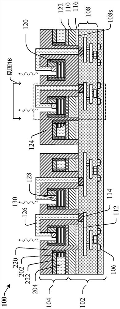
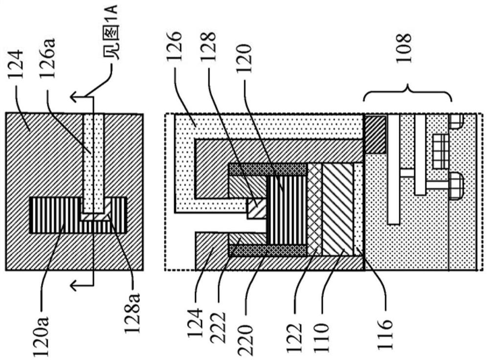
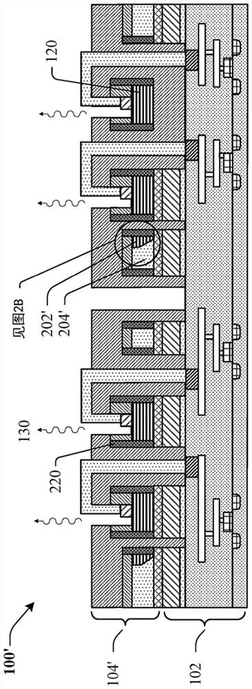
[0081] Many different implementation methods or examples are disclosed below to implement different features of the provided subject matter, and specific elements and embodiments of their arrangement are described below to illustrate the present invention. Of course, these examples are for illustration only, and should not limit the scope of the present invention. For example, it is mentioned in the description that the first feature is formed on the second feature, which includes the embodiment that the first feature is in direct contact with the second feature, and also includes other features between the first feature and the second feature. Embodiments of the features, that is, the first feature is not in direct contact with the second feature. In addition, repeated symbols or signs may be used in different embodiments, and these repetitions are only for the purpose of simply and clearly describing the present invention, and do not represent a specific relationship between...


PUM

PropertyMeasurementUnit
diameteraaaaaaaaaa

Abstract

A method for forming a semiconductor chip is provided, comprising: providing a silicon carrier wafer, which has a first surface and a second surface, wherein an epitaxial III-V group semiconductor region and an oxidized region are arranged on the first surface, and an epitaxial III-V group The semiconductor region and the oxide region have approximately the same height measured from the first side of the silicon carrier wafer, and the sidewalls of the epitaxial III-V group semiconductor region contact the sidewalls of the oxide region; formed on the top surface of the epitaxial III-V group semiconductor region and the oxide region Eutectic bonding layer; bonding CMOS wafer to eutectic bonding layer; subsequent removal of silicon carrier wafer; singulating CMOS wafer to form three-dimensional integrated circuits, both comprising CMOS substrate and III The ‑V optical device, the CMOS substrate and the III‑V optical device correspond to a part of the CMOS chip and the III‑V optical device, respectively.

Description

technical field [0001] Embodiments of the present invention relate to a semiconductor chip and a method for forming the same, and more particularly to a semiconductor chip for wafer-to-wafer bonding and a method for forming the same. Background technique [0002] It is well known that semiconductor chips are used in all kinds of electronic components and other devices. Today's widespread use of such chips, coupled with consumer demand for more powerful and smaller devices, has led chip manufacturers to continually reduce the physical size of chips and increase their functionality. To shrink chip footprints, manufacturers are increasingly pushing to achieve smaller feature sizes and die sizes, allowing more dies to fit within a given size wafer. To shrink the height of chips, manufacturers have worked hard to create three-dimensional or stacked integrated circuits (3DIC's). Existing methods of manufacturing these stacked chips, such as the pick-and-place method used to bond...

Claims


Application Information

Patent Timeline
Patent Type & Authority Patents(China)
IPC IPC(8): H01L21/18
CPCH01L21/187H01L27/15H01L27/156H01L33/62H01L21/185H01L21/8258H01L2224/18H01L33/0095H01L21/76251H01L21/28575H01L33/0093
Inventor 刘铭棋李汝谅蔡嘉雄陈逸群亚历山大·卡尼斯基余振华
Owner TAIWAN SEMICON MFG CO LTD
Features
  • R&D
  • Intellectual Property
  • Life Sciences
  • Materials
  • Tech Scout
  • Unparalleled Data Quality
  • Higher Quality Content
  • 60% Fewer Hallucinations
Learn More