Distance optimizing method of through silicon via (TSV) positions in three-dimensional (3D) integrated circuit automatic layout

An integrated circuit, automatic layout technology, applied in the direction of electrical digital data processing, special data processing applications, instruments, etc., can solve problems such as inability to process, and achieve the effect of avoiding too dense

Inactive Publication Date: 2012-09-12
BEIJING UNIV OF TECH
View PDF4 Cites 12 Cited by
  • Summary
  • Abstract
  • Description
  • Claims
  • Application Information

AI Technical Summary

Problems solved by technology

When processing and producing 3D integrated circuits, manufacturers cannot process layouts

Method used


Image

  • Distance optimizing method of through silicon via (TSV) positions in three-dimensional (3D) integrated circuit automatic layout
  • Distance optimizing method of through silicon via (TSV) positions in three-dimensional (3D) integrated circuit automatic layout
  • Distance optimizing method of through silicon via (TSV) positions in three-dimensional (3D) integrated circuit automatic layout

Examples


Embodiment Construction

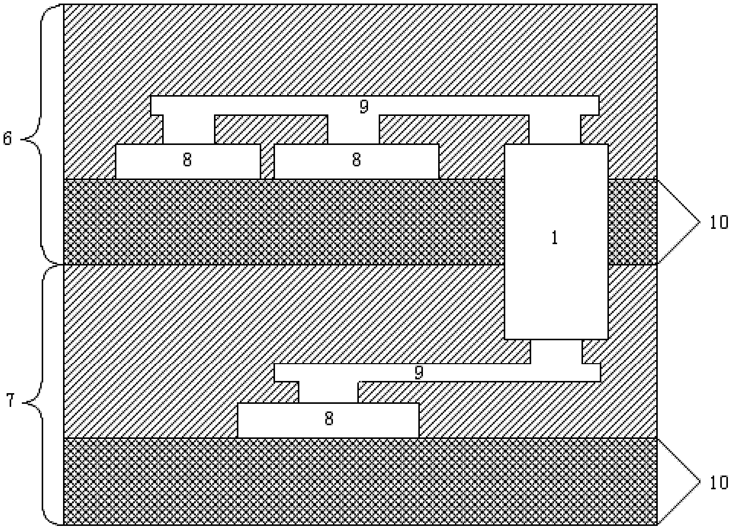
[0036] A 3D integrated circuit is a three-dimensional chip structure, each layer of which is a 2D chip, and the structure between any two layers is as follows: figure 1 As shown, the units 8 in the chip are arranged horizontally in the chip, and the units are the basic structure for signal communication in the circuit, and are connected by metal interconnection lines in the chip. The units in the adjacent two-layer chips need to be connected through TSV1. TSV1 is a via hole passing through the chip in the circuit, so that the upper and lower two-layer chips are connected. Therefore, TSV1 is a structure different from 2D circuits for 3D integrated circuits. Among them, in the 3D circuit, the upper chip is called the top chip, and the lower chip is called the bottom chip. These two layers of chips can be any two layers of adjacent chips in the 3D circuit.

[0037] The present invention is dedicated to optimizing the 3D integrated circuit layout whose TSV1 coordinates have been ...


PUM


Abstract

The invention discloses a distance optimizing method of through silicon via (TSV) positions in a three-dimensional (3D) integrated circuit automatic layout. The distance optimizing method has wide application to the field of design and manufacture of 3D integrated circuits. In a layout formed after initial locating of common 3D integrated circuit TSVs, the number of the TSVs is big, and distribution of the TSVs in the layout is dense, therefore a problem that the positions of the TSVs are too close occurs. When the 3D integrated circuit is manufactured and produced, manufacturers can not manufacture the layout where gaps of the TSVs are smaller than gap restrain of manufacture process. The method uses a distance method to optimize the gaps of the TSVs, an optimized layout is obtained so as to enable the gaps of the TSVs to meet process manufacture requirements, and manufacture can be finished. In the optimized TSV layout, distance of the TSVs is appropriate, working speed of the circuit can be increased, and crosstalk is reduced.

Description

field of invention [0001] The present invention generally relates to the design and manufacture of 3D integrated circuits, and more specifically, the present invention relates to a method for automatic layout in 3D integrated circuit design, which belongs to the field of circuit design. Background technique [0002] The design and manufacturing level of integrated circuits has been developing rapidly, and now hundreds of millions of transistors can be integrated on a single chip. More specifically, according to the description of Moore's Law, the advanced technology level has reached the nanometer level. Due to the increase in the number of transistors on a single chip, ordinary 2D integrated circuits will cause the problem of excessively long lines, which will reduce the operation speed of the circuit and increase power consumption. 3D integrated circuits can effectively reduce line length, improve computing speed, and reduce power consumption. [0003] 3D integrated circ...

Claims


Application Information

Patent Timeline
IPC IPC(8): G06F17/50
Inventor 侯立刚汪金辉白澍彭晓宏耿淑琴
Owner BEIJING UNIV OF TECH
Why Eureka
Try Eureka