3D Integrated Circuit and Methods of Forming Same

A technology of integrated circuits and dielectrics, applied in the field of 3D integrated circuits and their formation

Active Publication Date: 2015-04-29
TAIWAN SEMICON MFG CO LTD
View PDF3 Cites 15 Cited by
  • Summary
  • Abstract
  • Description
  • Claims
  • Application Information

AI Technical Summary

Problems solved by technology

Conversely, if the expanded volume of the metal pad is significantly greater tha

Method used


Image

  • 3D Integrated Circuit and Methods of Forming Same
  • 3D Integrated Circuit and Methods of Forming Same
  • 3D Integrated Circuit and Methods of Forming Same

Examples


Embodiment Construction

[0029] The making and using of various embodiments of the present disclosure are discussed in detail below. It should be appreciated, however, that the embodiments provide many applicable concepts that can be implemented in a wide variety of specific contexts. The specific embodiments discussed are illustrative, and do not limit the scope of the disclosure.

[0030] Packages including hybrid bonding and methods of forming such packages are provided according to various exemplary embodiments. Intermediate stages in forming such a package are shown. Variations of the embodiments are discussed. Like reference numerals are used to refer to like elements throughout the various drawings and throughout the illustrative embodiments.

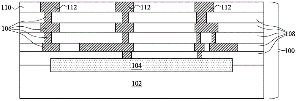
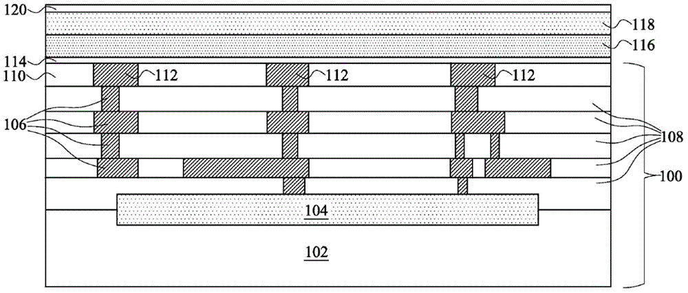
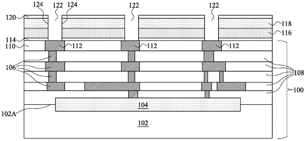
[0031] Figure 1 to Figure 5 Shown is a cross-sectional view of an intermediate stage in forming a packaged assembly according to some embodiments. refer to figure 1 , shows package assembly 100 . The package assembly 100 may include a device wafe...


PUM


Abstract

An integrated circuit structure includes a package component, which further includes a non-porous dielectric layer having a first porosity, and a porous dielectric layer over and contacting the non-porous dielectric layer, wherein the porous dielectric layer has a second porosity higher than the first porosity. A bond pad penetrates through the non-porous dielectric layer and the porous dielectric layer. A dielectric barrier layer is overlying, and in contact with, the porous dielectric layer. The bond pad is exposed through the dielectric barrier layer. The dielectric barrier layer has a planar top surface. The bond pad has a planar top surface higher than a bottom surface of the dielectric barrier layer.

Description

technical field [0001] The present invention generally relates to the field of semiconductor technology, and more specifically, relates to a 3D integrated circuit and a method for forming the same. Background technique [0002] In wafer-to-wafer bonding technology, various methods have been developed to bond two package components, such as wafers, together. Available bonding methods include fusion bonding, eutectic bonding, direct metal bonding, hybrid bonding, and the like. In fusion bonding, the oxide surface of a wafer is bonded to either the oxide surface or the silicon surface of another wafer. In eutectic bonding, two eutectic materials are brought together and a specific pressure and temperature are applied. Under different conditions, eutectic materials melt. The wafers are bonded together as the molten eutectic material solidifies. In direct metal-to-metal bonding, two metal pads are pressed against each other at elevated temperature and the interdiffusion of th...

Claims


Application Information

Patent Timeline
IPC IPC(8): H01L27/02H01L23/528H01L21/768H01L23/52
CPCH01L25/0657H01L2224/05547H01L2224/80357H01L23/291H01L23/293H01L24/05H01L24/08H01L24/80H01L2224/05624H01L2224/05647H01L2224/05684H01L2224/80097H01L2224/80201H01L2224/80895H01L2224/80896H01L2224/03616H01L2924/01322H01L23/562H01L2225/06513H01L2224/05124H01L2224/05147H01L2224/05655H01L23/3192H01L2224/80948H01L25/50H01L2224/8034H01L2924/00014H01L2924/00H01L24/06H01L24/89H01L2924/01029H01L25/043H01L24/10H01L25/0756H01L23/538H01L24/18H01L23/5385H01L21/76805H01L21/76883
Inventor 匡训冲朱彦璋萧清泰刘丙寅赵兰璘杜友伦蔡嘉雄陈晓萌
Owner TAIWAN SEMICON MFG CO LTD
Why Eureka
Try Eureka