3D integrated circuit and its manufacturing method

An integrated circuit, 3D technology, applied in the direction of circuit, semiconductor/solid-state device manufacturing, electrical components, etc., can solve problems such as damage, failure, integrated circuit dielectric layer and through-silicon hole defects, and achieve the effect of avoiding damage

Active Publication Date: 2011-11-30
INST OF MICROELECTRONICS CHINESE ACAD OF SCI
View PDF2 Cites 13 Cited by
  • Summary
  • Abstract
  • Description
  • Claims
  • Application Information

AI Technical Summary

Problems solved by technology

[0002] In the manufacturing process of integrated circuits, metal ions such as Cu, Fe, and Na ions from through-silicon vias (through-Si-via, TSV), interconnect structures, or metal electrodes of semiconductor devices can easily diffuse into transistor structures and interconnect structure, resulting in degradation of integrated c

Method used


Image

  • 3D integrated circuit and its manufacturing method
  • 3D integrated circuit and its manufacturing method
  • 3D integrated circuit and its manufacturing method

Examples


Embodiment Construction

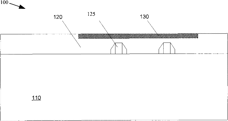
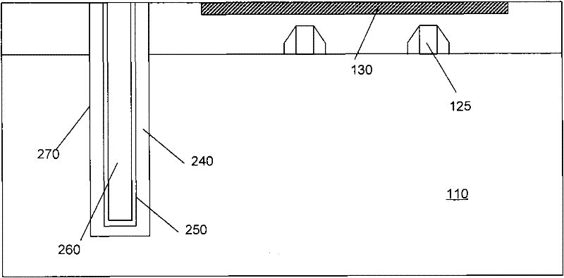
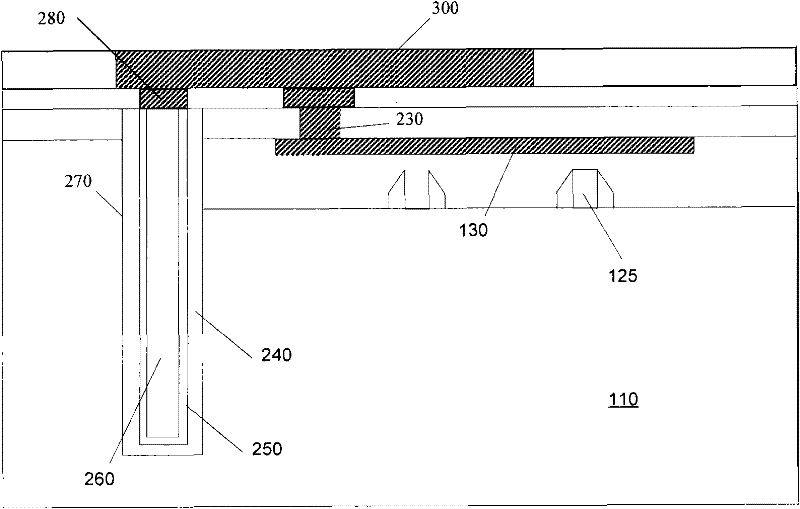
[0015] The disclosure below provides many different embodiments or examples to realize the technical solution provided by the present invention. Although components and arrangements of specific examples are described below, they are examples only and are not intended to limit the invention.

[0016] Furthermore, the present invention may repeat reference numerals and / or letters in different embodiments. This repetition is for simplicity and clarity and does not in itself indicate a relationship between the various embodiments and / or arrangements discussed.

[0017] The present invention provides examples of various specific processes and / or materials, however, alternative applications of other processes and / or other materials that can be realized by those skilled in the art obviously do not depart from the scope of the present invention. It should be emphasized that the boundaries of various regions described in this document include necessary extensions due to process or pro...


PUM


Abstract

The invention provides a 3D (three-dimensional) IC (integrated circuit) and a manufacturing method thereof. The circuit comprises a semiconductor substrate, a semiconductor device, a silicon through hole, an interconnection structure and a diffusion trapping region, wherein the semiconductor device is formed on the upper surface of the semiconductor substrate; the silicon through hole penetrates through the semiconductor substrate and comprises an insulating layer for covering the side walls of the silicon through hole and a conducting material filled in the insulating layer; the interconnection structure is used for connecting the semiconductor device with the silicon through hole; and the diffusion trapping region is formed on the lower surface of the semiconductor substrate. The manufacturing method is applicable to manufacturing of 3D integrated circuits.

Description

technical field [0001] The invention relates to the field of integrated circuit manufacturing, in particular to an integrated circuit with a diffusion trap layer and a manufacturing method thereof. Background technique [0002] In the manufacturing process of integrated circuits, metal ions such as Cu, Fe, and Na ions from through-silicon vias (through-Si-via, TSV), interconnect structures, or metal electrodes of semiconductor devices can easily diffuse into transistor structures and In the interconnection structure, the performance of the integrated circuit is degraded, or even malfunctioned. [0003] The method of directly implanting ions into the integrated circuit structure can be used to trap metal ions, but the implanted ions may enter areas other than the target area, especially may cause defects and damage to the dielectric layer and through-silicon holes in the integrated circuit. . Contents of the invention [0004] In order to solve the above problems, accordi...

Claims


Application Information

Patent Timeline
IPC IPC(8): H01L27/02H01L23/485H01L21/768H01L21/265H01L21/304
CPCH01L23/481H01L2924/0002H01L21/76898
Inventor 朱慧珑
Owner INST OF MICROELECTRONICS CHINESE ACAD OF SCI
Why Eureka
Try Eureka