Method and carrier for handling a substrate

Inactive Publication Date: 2015-03-26
APPLIED MICROENG
View PDF0 Cites 16 Cited by
  • Summary
  • Abstract
  • Description
  • Claims
  • Application Information

AI Technical Summary

Benefits of technology

[0068]At least one of the platens may comprise a heater for increasing the temperature of a carrier and s

Problems solved by technology

A thinned wafer, for example <100 μm in thickness, will be easily damaged at its edge.
Very thin substrates, such as ˜50 μm, become flexible and may therefore be difficult to process.
A further problem with using adhesive to bond the substrate to the carrier is that it is difficult to precisely control the thickness of the adhesive evenly across the carrier surface and maintain this even thickness as the substrate is brought into contact.
If this unevenness is present when a substrate is sent for thinning the resultant thinned substrate may have a wedge profile with one side thicker than the other which may result in an unusable substrate.
This unnecessarily subjects features on the surface of the substrate to further processing including solvent cleaning.

Method used


Image

  • Method and carrier for handling a substrate
  • Method and carrier for handling a substrate
  • Method and carrier for handling a substrate

Examples


Embodiment Construction

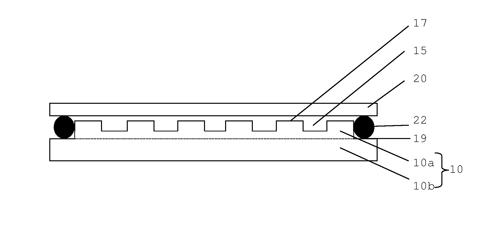
[0084]There are many integrated circuit, MEMS, and III-V fabrication processes that require thinning of substrates or handling of thinned substrates or wafers during processing. For example, after fabricating devices on a front side of a wafer or substrate it is often necessary to perform processing on the back side of the wafer or substrate. For example, back side thinning. Conventional techniques bond the wafer or substrate to a carrier using adhesive. The wafer or substrate is then debonded from the carrier after backside processing has been performed.

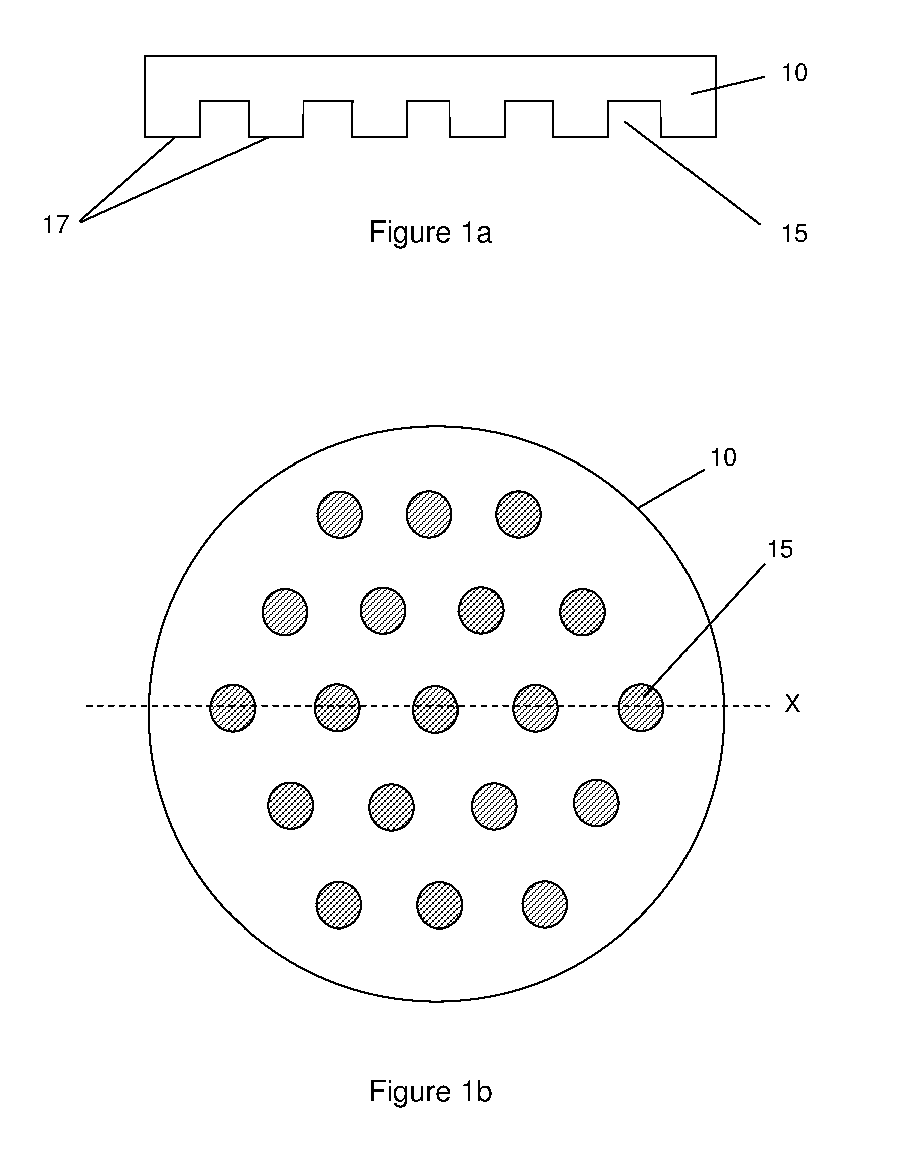
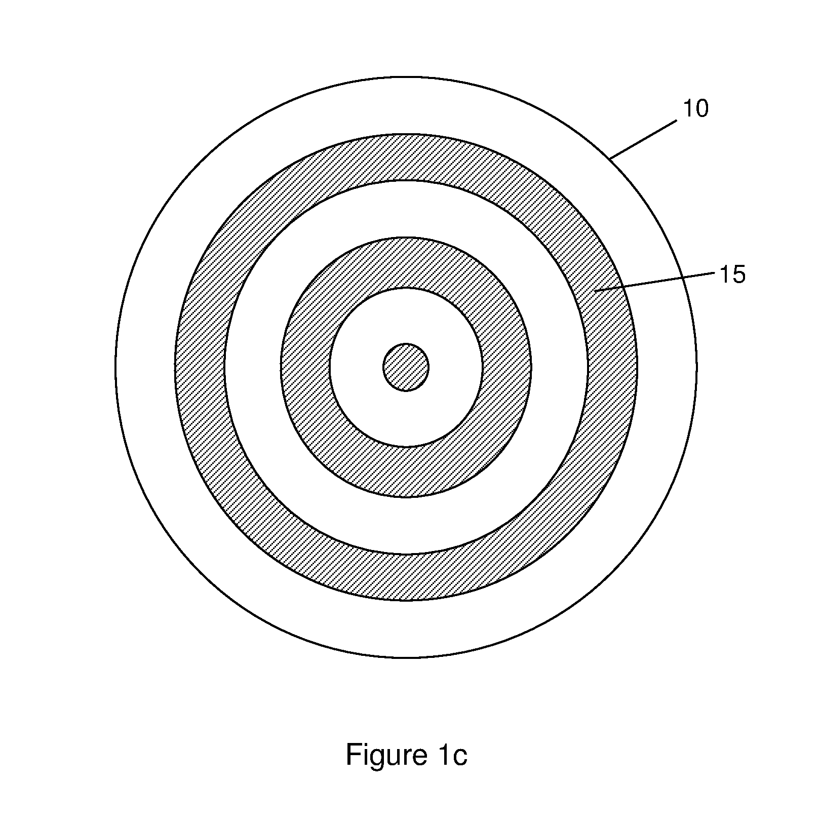
[0085]FIGS. 1a and 1b show a carrier 10 for supporting a wafer or substrate during processing. In the following discussion we use the term wafer or process wafer, which normally refers to a semiconductor substrate, but other substrates such as glass may also be processed in this way.

[0086]The carrier 10 is of similar plan dimension to a process wafer to be processed or handled. For example, as shown in FIG. 1b the carrier may be cir...


PUM


Abstract

There is disclosed a carrier and method for handling and/or transport of a substrate, such as during processing of the substrate, for example, back-thinning. The carrier and method provide support for the substrate. The process is particularly suited to thinning of substrates for use in 3D integrated circuits. The carrier comprises: a contact surface with one or more recesses therein for trapping a volume when the contact surface is brought towards the substrate, the contact surface for supporting the substrate; a sealing surface at the periphery of the contact surface and offset from the contact surface; and the sealing member seating on the sealing surface and arranged to be compressed to form a seal to the substrate when a substrate is in contact with the contact surface, the seal sealing the trapped volume between the substrate and carrier.

Description

TECHNICAL FIELD[0001]The present invention relates to a method and carrier for handling a substrate for transport and / or processing. The method is particularly suited to handling and support of substrates where backside processing such as thinning is performed.BACKGROUND ART[0002]There are many integrated circuit, MEMS, and III-V fabrication processes that require thinning of substrates or handling of thinned substrates or wafers. Substrates or wafers thinned to around 100 μm or less are fragile and may even be flexible such that during further processing steps they require support to prevent flexing or breakage.[0003]Current techniques for providing structural rigidity require the substrate or wafer to be mounted on a temporary carrier during the thinning process or for post-thinning processing. The substrate or wafer is bonded to a carrier wafer using an adhesive. The adhesive is applied to the carrier wafer, such as by spinning on to the surface followed by a partial bake. The ad...

Claims


Application Information

Patent Timeline
IPC IPC(8): H01L21/683
CPCH01L21/6838
Inventor ROGERS, TONYSANTILLI, ROB
Owner APPLIED MICROENG
Why Eureka
Try Eureka