Chip packaging structure, manufacturing method thereof and electronic equipment

A chip packaging structure and chip technology, applied in circuits, electrical components, electrical solid devices, etc., can solve the problems of large thickness of the chip packaging structure

Inactive Publication Date: 2019-03-05
HUAWEI TECH CO LTD
View PDF3 Cites 18 Cited by
  • Summary
  • Abstract
  • Description
  • Claims
  • Application Information

AI Technical Summary

Problems solved by technology

[0005] The present application provides a chip packaging structure and its manufacturing method,...

Method used


Image

  • Chip packaging structure, manufacturing method thereof and electronic equipment
  • Chip packaging structure, manufacturing method thereof and electronic equipment
  • Chip packaging structure, manufacturing method thereof and electronic equipment

Examples


Embodiment Construction

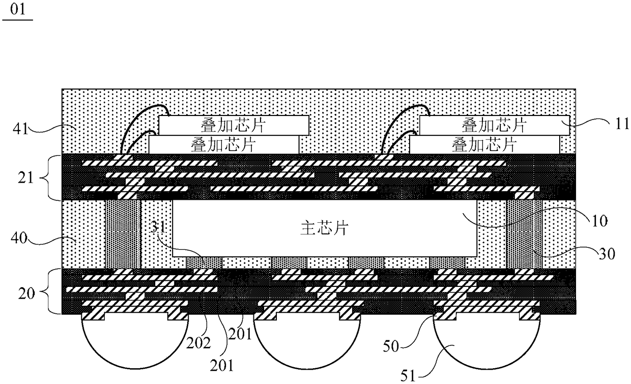
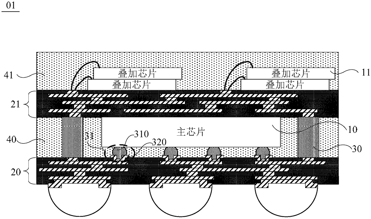
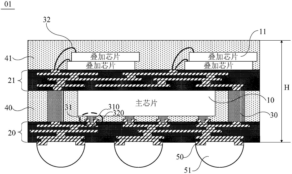
[0031] This application provides a chip packaging structure 01, such as figure 1 As shown, it includes: a main chip 10 , a first redistribution layer 20 , a second redistribution layer 21 , a first electrical connector 30 and an overlay chip 11 .

[0032] It should be noted that the present application does not limit the number of the above-mentioned main chips 10 and stacked chips 11 . In addition, the above-mentioned main chip 10 and stacked chip 11 generally have different functions. For example, the main chip 10 may be a logic chip, and the superimposed chip 11 may be a memory chip. In this case, when the above-mentioned chip package structure 01 has a plurality of logic chips serving as the main chips 10, the above-mentioned multiple main chips 10 may be located on the same plane and arranged at intervals. In this case, the above-mentioned first electrical connecting member 30 may or may not be provided between two adjacent main chips 10 . Those skilled in the art can ...


PUM


Abstract

The invention discloses a chip packaging structure, a manufacturing method and electronic equipment, relates to the technical field of electronic packaging, and solves the problem that the thickness of the chip packaging structure is relatively high. Through the specific scheme, the chip packaging structure comprises a main chip, a first re-wiring layer, a second re-wiring layer, a first electronic connecting piece and an overlaying chip, wherein the first re-wiring layer is arranged on the active surface of the main chip, and is electrically connected with the main chip; the second re-wiringlayer is arranged on the back surface of the main chip, and is in contact with the back of the main chip; the first electric connecting piece is arranged between the first re-wiring layer and the second re-wiring layer, and the first electric connecting piece is used for electrically connecting the first re-wiring layer and the second re-wiring layer; and the overlaying chip is arranged on the side, away from the main chip, of the second re-wiring layer, and is electrically connected with the second re-wiring layer. The chip packaging structure provided by the invention is used for being connected with a circuit board inside the electronic equipment.

Description

technical field [0001] The present application relates to the technical field of electronic packaging, in particular to a chip packaging structure, a manufacturing method thereof, and electronic equipment. Background technique [0002] With the rapid development of wireless communication, automotive electronics and other consumer electronic products, electronic devices are developing in the direction of multi-function. Based on this, in the prior art, when manufacturing the above-mentioned electronic device, chips with different functions are usually packaged separately, and then integrated, and the integrated components are arranged in the above-mentioned electronic device. [0003] Currently, the packaging and integration technology adopted is a package on package (Package on Package, POP) technology. Specifically, a chip package structure formed by the stacking packaging technology includes a lower package and an upper package formed by stacking. Wherein, the lower packa...

Claims


Application Information

Patent Timeline
IPC IPC(8): H01L25/18H01L23/538H01L23/31H01L23/367H01L21/98
CPCH01L23/3107H01L23/367H01L23/5383H01L25/18H01L25/50H01L2224/16225H01L2224/48091H01L2224/48227H01L2924/15311H01L2924/181H01L21/768H01L23/31H01L23/538H01L2924/00012H01L2924/00014
Inventor 王双福
Owner HUAWEI TECH CO LTD
Why Eureka
Try Eureka