Pixel structure and display panel comprising said pixel structure
A pixel structure and pixel technology, applied in the direction of static indicators, instruments, semiconductor devices, etc., can solve the problems of non-full-color display and distortion of display effect, and achieve the effect of balancing life, changing decay too fast, and reducing difficulty
- Summary
- Abstract
- Description
- Claims
- Application Information
AI Technical Summary
Problems solved by technology
Method used
Image

Examples
Embodiment 1
[0042] Figure 4 It is a schematic diagram of pixel arrangement of the display panel in Embodiment 1 of the present invention. Here, the X direction is referred to as the row direction (horizontal direction), and the Y direction is referred to as the column direction (vertical direction). For simplicity, only a part of the OLED display panel is shown in the drawings, and the number of pixels in an actual product is not limited to this, and the number of pixel units can be changed accordingly according to actual display requirements.
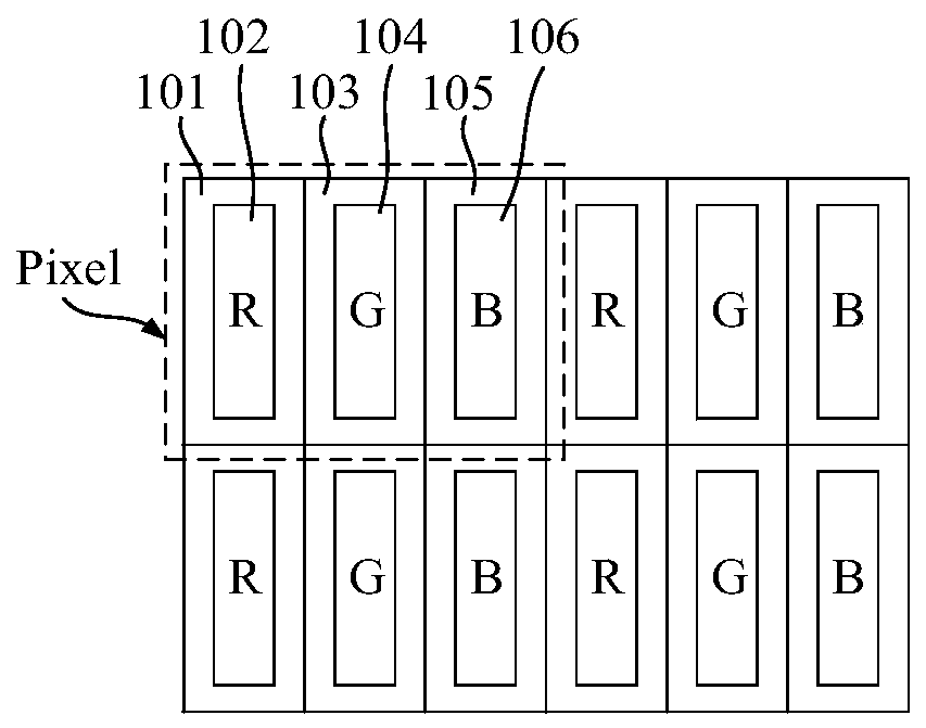
[0043] like Figure 4 As shown, the pixel structure of the display panel includes a plurality of pixel units arranged in an array, and each pixel unit includes a first sub-pixel 301, a second sub-pixel 303, and a third sub-pixel 305, and the first sub-pixel 301 and The second sub-pixels 303 are arranged in one column, and the third sub-pixels 305 are arranged in another column. The total size L1 of the first sub-pixels 301 and the second sub-pi...
Embodiment 2
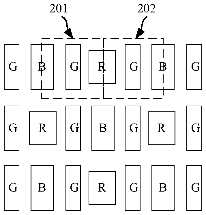
[0053] Image 6 It is a schematic diagram of pixel arrangement of the display panel shown in Embodiment 2 of the present invention. like Image 6As shown, the pixel structure of the display panel includes a plurality of pixel units arranged in an array, and each pixel unit includes a first sub-pixel 301, a second sub-pixel 303, and a third sub-pixel 305, and the first sub-pixel 301 and The second sub-pixels 303 are arranged in one column, and the third sub-pixels 305 are arranged in another column. The total size L1 of the first sub-pixels 301 and the second sub-pixels 303 along the column direction (that is, the first sub-pixels 301 and the second sub-pixels 301 The sum of the sizes of the two sub-pixels 303 along the column direction) is larger than the size L2 of the third sub-pixel 305 along the column direction, and the arrangement structure of all pixel units in the same row is the same, and each pixel unit is flipped along the row direction (itself left and right The ...
Embodiment 3
[0057] Figure 8 It is a schematic diagram of pixel arrangement of the display panel shown in Embodiment 3 of the present invention. like Figure 8 As shown, the pixel structure of the display panel includes a plurality of pixel units arranged in an array, and each pixel unit includes a first sub-pixel 301, a second sub-pixel 303, and a third sub-pixel 305, and the first sub-pixel 301 and The second sub-pixels 303 are arranged in one column, and the third sub-pixels 305 are arranged in another column. The total size L1 of the first sub-pixels 301 and the second sub-pixels 303 along the column direction (that is, the first sub-pixels 301 and the second sub-pixels 301 The sum of the sizes of the two sub-pixels 303 along the column direction) is larger than the size L2 of the third sub-pixel 305 along the column direction, and the arrangement structure of all pixel units in the same row is the same, and each pixel unit is flipped along the row direction (itself left and right T...
PUM
 Abstract
Description
Claims
Application Information
 - R&D
- Intellectual Property
- Life Sciences
- Materials
- Tech Scout
- Unparalleled Data Quality
- Higher Quality Content
- 60% Fewer Hallucinations
Browse by: Latest US Patents, China's latest patents, Technical Efficacy Thesaurus, Application Domain, Technology Topic, Popular Technical Reports.
© 2025 PatSnap. All rights reserved.Legal|Privacy policy|Modern Slavery Act Transparency Statement|Sitemap|About US| Contact US: help@patsnap.com