Automatic optical detection device and method applicable to artificial intelligence detection PCB

A technology of automatic optical detection and automatic detection device, which is used in measurement devices, material analysis by optical means, scientific instruments, etc., can solve problems such as low efficiency of detection systems, and achieve the effect of improving work efficiency and reducing costs.

Pending Publication Date: 2019-03-08
SUZHOU GPOWER
View PDF0 Cites 9 Cited by
  • Summary
  • Abstract
  • Description
  • Claims
  • Application Information

AI Technical Summary

Problems solved by technology

[0002] With the rapid development of optoelectronics, communications, computers, machinery, materials and other industries, the industry of PCB and IC substrates is also developing rapidly. In modern electronic and communication products, PCBs and IC substrates can be seen almost everywhere, as small as a chip , large to ultra-large integrated PCB, PCB and IC carrier board are the

Method used


Image

  • Automatic optical detection device and method applicable to artificial intelligence detection PCB
  • Automatic optical detection device and method applicable to artificial intelligence detection PCB

Examples


Embodiment

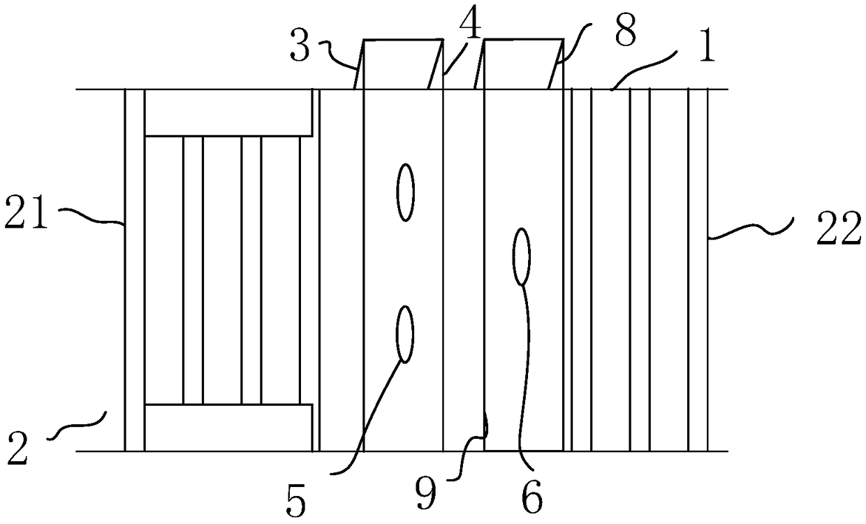
[0034] The invention can make the object under test realize the gray-scale image and color image under the action of the scanning camera and the photographing camera to detect whether there is a defect in the object under test, and the defect of the object under test can be clearly known through the gray-scale image, and its Carry out position confirmation, and the position of the defect of the object under test can be enlarged through the color image to confirm the defect, so as to repair it. Such as figure 1 As shown, it includes a frame 1, the frame 1 is provided with a transfer platform 2, and the transfer platform 2 is provided with a feed section 21 and a discharge section 22, both of which are located on the same transfer platform 2. The frame 1 is provided with a first bracket 3 and a second mobile bracket 8, and the first bracket and the second mobile bracket 8 are all horizontally mounted on the transmission platform 2, and are vertically arranged with the transmissi...

Embodiment 1

[0037] On the contact of above-mentioned embodiment, aim at the deficiency of photographing camera 6, increase a photographing camera to make up for the possibility that the precision is not high, this structure is also relatively simple, by increasing one on the rear end of original photographing camera identical with the original As for the camera, both of them are arranged on the same axis, and the requirement of precision is realized through the second camera.

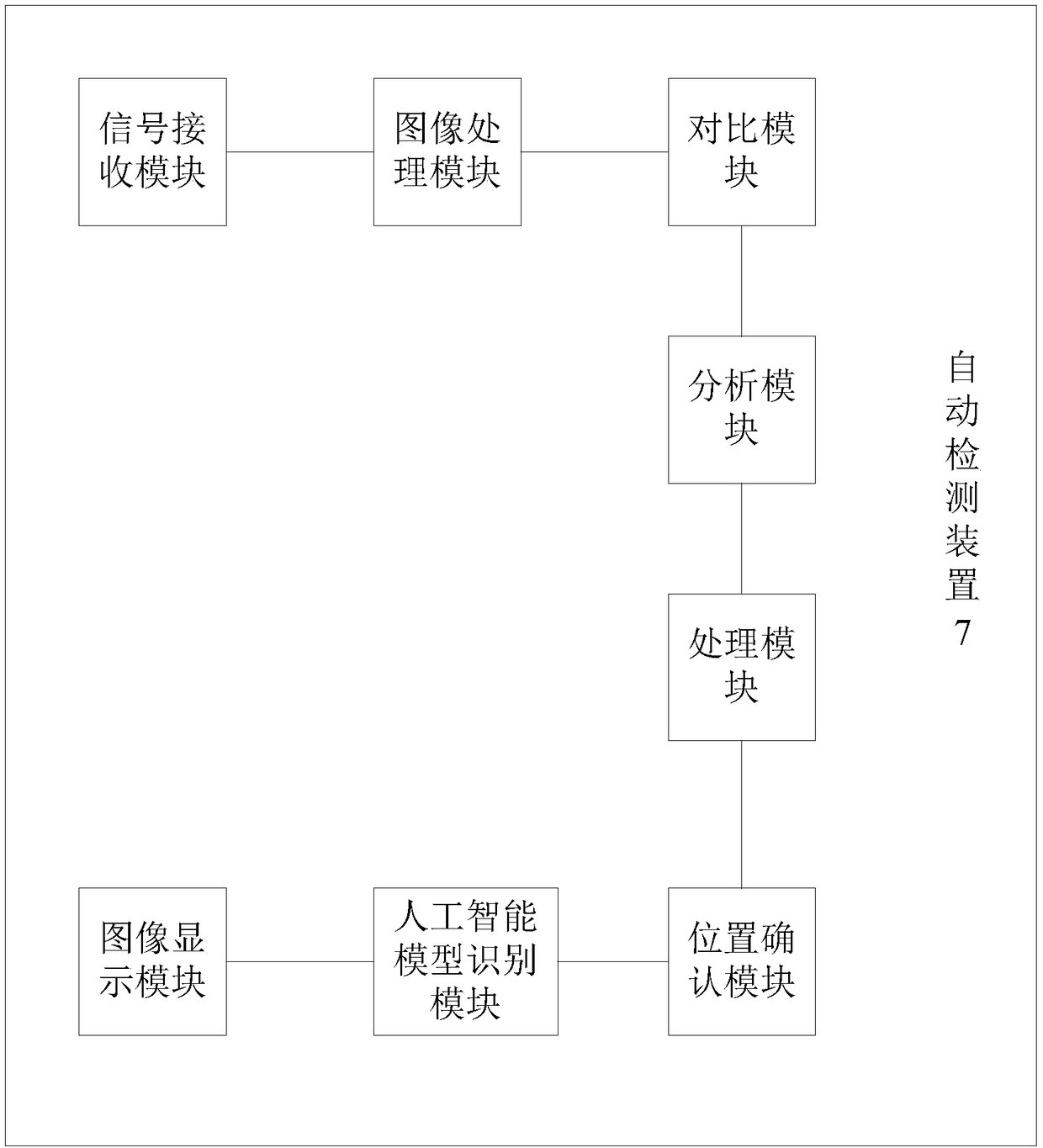
[0038]In the present invention, the scanning of the scanning camera 5 and the photographing of the photographing camera 6 are set synchronously, so as to ensure that the scanning camera and the photographing camera can simultaneously collect the same object to be measured and ensure its accuracy. The main purpose of one or several camera cameras is to make the working time of the scanning camera and the camera camera tend to be consistent, and at the same time automatically mark according to the recognition results ...


PUM


Abstract

The invention relates to an automatic optical detection device and method applicable to an artificial intelligence detection PCB. The automatic optical detection device comprises a machine frame, wherein a transmission platform is arranged on the machine frame; a feeding section and a discharging section are arranged on the transmission platform; a first support frame is arranged on a feeding end;a scanning camera is arranged on the first support frame; a second moving support frame is also arranged on the discharging section; one or a plurality of photo taking cameras are connected onto thesecond moving support frame; the scanning camera and the photo taking camera are arranged in a matched way; the scanning camera and the photo taking camera are connected with an automatic detection and artificial intelligence recognition device; an artificial intelligence software part operates by using a special host. The fully automatic detection can be realized; the work efficiency is improved.

Description

technical field [0001] The invention relates to an automatic optical detection device suitable for artificial intelligence detection of PCBs, in particular to an automatic optical detection device suitable for artificial intelligence detection of PCBs and a method thereof. Background technique [0002] With the rapid development of optoelectronics, communications, computers, machinery, materials and other industries, the industry of PCB and IC substrates is also developing rapidly. In modern electronic and communication products, PCBs and IC substrates can be seen almost everywhere, as small as a chip , large to ultra-large integrated PCB, PCB and IC carrier board are the pillar industries in the current and future electronics industry. At the same time, the rapid development of PCB and IC carrier board industry puts forward higher requirements for the quality of PCB and IC carrier board. To produce high-quality PCBs and IC substrates, optical inspection must be performed on...

Claims


Application Information

Patent Timeline
IPC IPC(8): G01N21/956
CPCG01N21/956G01N2021/95638
Inventor 吴勇军李延奇盛宇清
Owner SUZHOU GPOWER
Why Eureka
Try Eureka