
LED device and manufacturing method thereof

A technology of LED devices and manufacturing methods, which is applied in the direction of semiconductor devices, electrical components, circuits, etc., can solve the problems of uncontrollable enhancement of the surface of light-transmitting colloids, poor surface molding quality, and large light output angles, etc., to achieve good processing convenience, The effect of high processing efficiency

Pending Publication Date: 2019-03-08
FOSHAN NATIONSTAR OPTOELECTRONICS CO LTD
View PDF1 Cites 2 Cited by
  • Summary
  • Abstract
  • Description
  • Claims
  • Application Information

AI Technical Summary

Problems solved by technology

[0004] In the step of removing the light-shielding material to expose the top of the light-transmitting colloid to form the light-transmitting part, this patent is realized by grinding and other methods. Due to the existence of processing errors, it is difficult to remove the light-shielding material completely and accurately in each process It does not affect the light-transmitting colloid. Therefore, every time the process of removing the light-shielding material is always accompanied by cutting of the light-transmitting colloid, the surface molding quality is poor, and the specific performance is that the optical path is on the surface of the light-transmitting colloid. The uncontrollability is enhanced, which is not conducive to the formation of a light source with a stable luminous angle;
[0005] In addition, for the light-emitting diode structure in this patent, limited by the manufacturing method, since the top surface of the light-transmitting colloid and the top surface of the black glue are always flat, resulting in a large light-emitting angle

Method used


Image

  • LED device and manufacturing method thereof
  • LED device and manufacturing method thereof
  • LED device and manufacturing method thereof

Examples


Embodiment 1

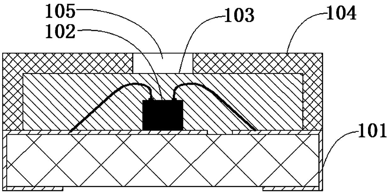
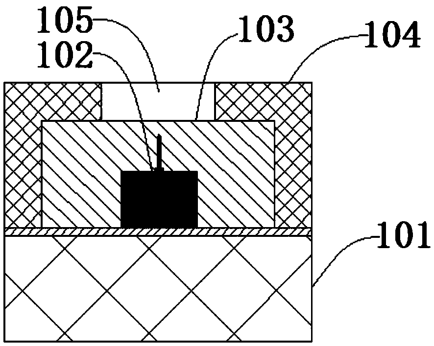
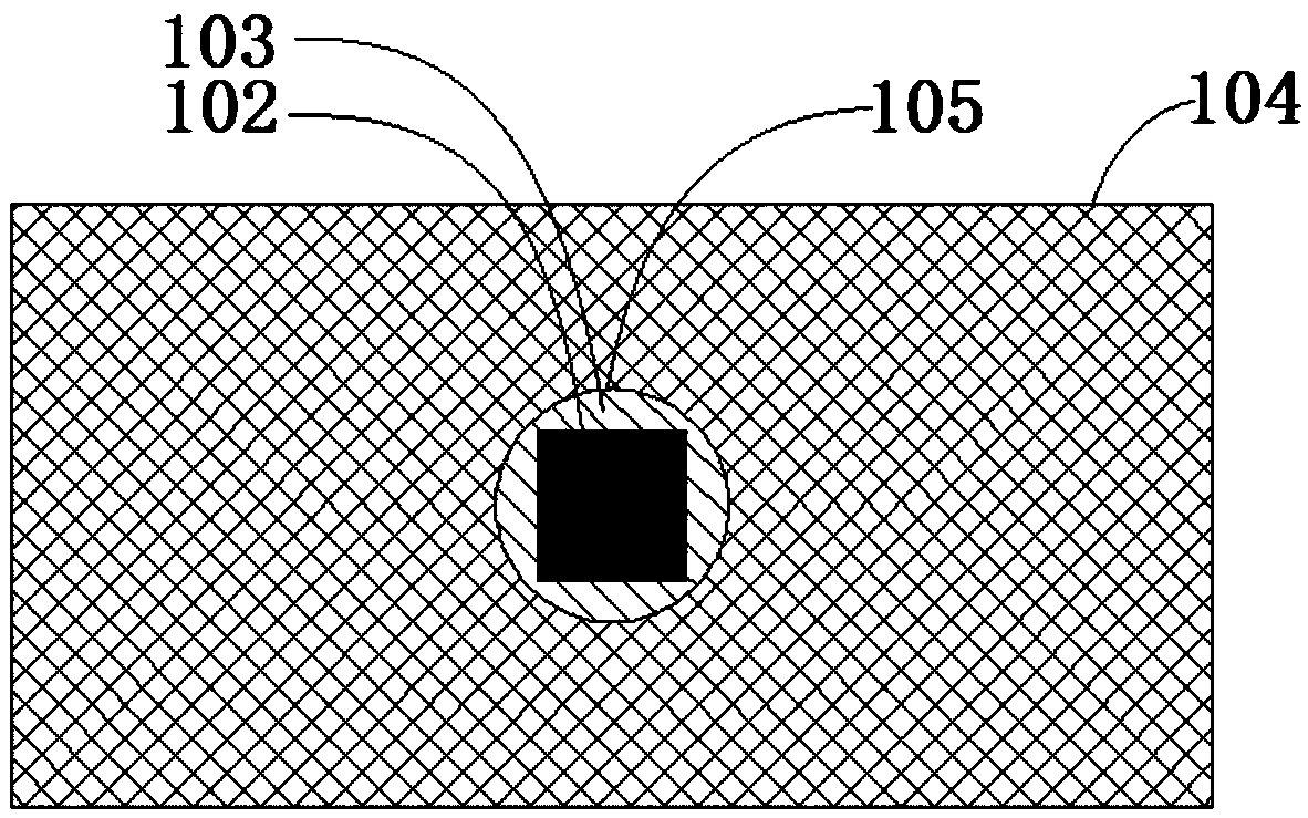
[0069] figure 1 Shows a front cross-sectional view of an LED device according to an embodiment of the present invention, figure 2 shows a side cross-sectional view of an LED device according to an embodiment of the present invention, image 3 A top view of an LED device according to an embodiment of the present invention is shown. The LED device of the embodiment of the present invention includes a substrate unit 101 , a light-transmitting unit 103 , a light-shielding unit 104 and a light-emitting unit 102 .

[0070] Specifically, the substrate unit 101 is a rectangular structure, the light-emitting unit 102 is fixed in the middle of the substrate unit 101, the light-transmitting unit 103 covers the light-emitting unit 102, and is connected and fixed with the substrate unit 101; the light-shielding unit 104 covers the transparent The periphery of the light unit 103, the four sides are respectively perpendicular to the substrate unit 101, and the top surface is parallel to t...

Embodiment 2

[0073] Figure 5 A schematic diagram of the principle of the optical path of the LED device according to the embodiment of the present invention is shown. In a specific implementation, in order to further enhance the concentration of light and reduce the light exit angle, the contact surface between the light-transmitting unit and the light-transmitting part can be designed as a concave surface 501 that is sunken toward the direction of the light-emitting unit. The concave surface 501 has a certain converging effect on the light emitted from the light emitting unit. With the accompanying drawing in embodiment one Figure 4 For reference, the light originally blocked by the light-shielding inner wall in Embodiment 1 can be transmitted through the light-transmitting part after being converged by the concave surface 501. Compared with the top surface of the light-transmitting unit being a plane, under the same circumstances, the light-transmitting part The intensity of the ligh...

Embodiment 3

[0075] In Embodiments 1 and 2, the light-transmitting part is arranged on the top surface of the light-shielding unit, that is, the light-transmitting part is arranged on the top of the light-transmitting unit facing the light-emitting surface of the light-emitting unit, so that the light emitted by the light-emitting unit can only be emitted from the top surface. It penetrates through the light-transmitting part, so as to realize the purpose of controlling the light direction.

[0076] Specifically, it is also possible to arrange the light-transmitting part on the side of the light-shielding unit.

[0077] Figure 6 Shows a front cross-sectional view of an LED device according to an embodiment of the present invention, Figure 7 A side cross-sectional view of an LED device according to an embodiment of the present invention is shown. Specifically, in the embodiment of the present invention, the arrangement form of the substrate unit 101, the light-emitting unit 102, the lig...


PUM


Abstract

The invention provides an LED device and a manufacturing method thereof. The LED device comprises a substrate unit, a light emitting unit, a light transmitting unit and a light shielding unit; the light emitting unit is fixed on the substrate unit, and the light transmitting unit is covered on the periphery of the light emitting unit; and a light transmitting portion for allowing the light of thelight emitting unit to pass through is arranged at the outside of the surface of the light transmitting unit in advance, and the light shielding unit covers the rest positions excluding the light transmitting portion on the surface of the light transmitting unit. The light emitting direction of the LED device can be controlled as needed through a light transmitting hole on the light shielding unit, so that the practicability is good. The manufacturing method of the LED device comprises: forming the light transmitting units and the light shielding units of a plurality of LED devices in one injection molding process by using a light transmitting layer mould and a light shielding layer mould, so that the processing efficiency is higher; and by using a cutter cutting mode and by reasonably setting the cutting track, the cutting object and the cutting depth of a cutter, a light transmitting layer, a light shielding layer and a substrate can be efficiently separated.

Description

technical field [0001] The invention relates to the field of LED devices, in particular to an LED device and a manufacturing method thereof. Background technique [0002] Patent No. CN201310116168.4, the patent titled "Light Emitting Diode Packaging Structure and Its Manufacturing Method" discloses a light emitting diode packaging structure and its manufacturing method. In specific implementation, the manufacturing method of the light-emitting diode packaging structure described in this patent has the following disadvantages: [0003] In the step of coating the light-emitting element with the light-transmitting colloid, each light-transmitting colloid is set separately and formed by compression molding. In actual processing, it is necessary to use a multi-cavity mold for compression molding. Multi-cavity The cost of the body mold and the purchase cost of the corresponding press are relatively high, and the molding is difficult; [0004] In the step of removing the light-sh...

Claims


Application Information

Patent Timeline
Patent Type & Authority Applications(China)
IPC IPC(8): H01L33/48H01L33/58H01L33/00
CPCH01L33/005H01L33/48H01L33/58
Inventor 陆紫珊王海军李国华
Owner FOSHAN NATIONSTAR OPTOELECTRONICS CO LTD
Learn More