Supercharge Your Innovation With Domain-Expert AI Agents!

Interface unit, interface module with interface unit, and chip

A chip and output interface technology, applied in the direction of logic circuit interface device, logic circuit connection/interface layout, electrical components, etc., can solve the problem that the same form of interface unit cannot be used

Active Publication Date: 2019-03-26
HUAWEI TECH CO LTD
View PDF3 Cites 4 Cited by
  • Summary
  • Abstract
  • Description
  • Claims
  • Application Information

AI Technical Summary

Problems solved by technology

[0008] The application provides an interface unit, an interface module and a chip with the interface unit, to solve the problem that the two packaging methods of TSV and MCM cannot use the same form of interface unit

Method used


Image

  • Interface unit, interface module with interface unit, and chip
  • Interface unit, interface module with interface unit, and chip
  • Interface unit, interface module with interface unit, and chip

Examples


Embodiment Construction

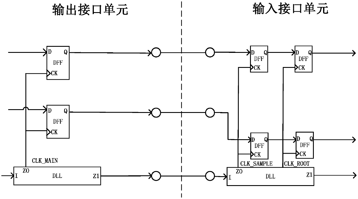
[0088] Figure 3a A schematic structural diagram of an output interface unit provided for this embodiment, including a first D flip-flop 1, a second D flip-flop 2, a splitter 3, a first multiplexer 4, and a second multiplexer 5 , the first clock generator 6 and the first controller 401. The input terminal D1 of the first D flip-flop 1 is the first input terminal of the output interface unit. The output terminal Q1 of the first D flip-flop 1 is connected to the input terminal I3 of the splitter 3 . The first output terminal Z30 of the splitter 3 is the first output terminal of the output interface unit. The second output terminal Z31 of the splitter 3 is connected to the first input terminal I40 of the first multiplexer 4 . The input terminal D2 of the second D flip-flop 2 is the second input terminal of the output interface unit. The output terminal Q2 of the second D flip-flop 2 is connected to the second input terminal I41 of the first multiplexer 4 . The output Z4 of t...


PUM


Abstract

The present application provides an output interface unit, an interface module with the interface unit, and a chip. The output interface unit comprises a first D trigger, a second D trigger, a splitter, a first multiplexer and a second multiplexer. The present application also provides a corresponding input interface unit, an interface module with the interface unit, and a chip. The input interface unit comprises a third D trigger, a fourth D trigger, a fifth D trigger and a third multiplexer. The output interface unit and the input interface unit control, by means of controlling a signal value of a routing signal, output states and input states of the splitter and the multiplexers, so that two packaging modes can be adopted in the same output interface unit or input interface unit, i.e. the two packaging modes of the TSV and the MCM can be compatible with each other in the same output interface unit or input interface unit.

Description

technical field [0001] The present application relates to the technical field of integrated circuits, and in particular to an interface unit, an interface module and a chip having the interface unit. Background technique [0002] Chip packaging usually integrates multiple bare chips (DIE) with other components into a complete chip through a specific method. The main packaging methods include through silicon via technology (through silicon via, TSV) and multi-chip packaging technology (multi chip package, MCP) two. Among them, TSV refers to the packaging method that realizes the signal connection between different layers in the chip through perforation, and MCM refers to the packaging method that realizes the signal connection between different layers in the chip by expanding and superimposing the die. [0003] The schematic diagram of the longitudinal section structure of the chip obtained by TSV packaging is as follows: Figure 1a As shown, in this chip, a micro-bump layer...

Claims


Application Information

Patent Timeline
IPC IPC(8): H03K19/0175H01L23/538
CPCH01L23/5381H03K19/017509H03K19/0175H01L23/538H01L25/065H01L2224/16227H01L2924/15311H01L2924/15192
Inventor 信恒超季秉武周昔平
Owner HUAWEI TECH CO LTD
Features
  • R&D
  • Intellectual Property
  • Life Sciences
  • Materials
  • Tech Scout
  • Unparalleled Data Quality
  • Higher Quality Content
  • 60% Fewer Hallucinations
Learn More