
Multispectral TDI (Time Delayed and Integration) imaging method and device

An imaging method and multi-spectral technology, applied in image communication, solid-state image signal generator, television, etc., can solve the problems that charges cannot be stored for a long time, TDICMOS devices are not easy to obtain, etc., and achieve the effect of high imaging accuracy

Inactive Publication Date: 2019-04-16
CHANGCHUN INST OF OPTICS FINE MECHANICS & PHYSICS CHINESE ACAD OF SCI
View PDF2 Cites 11 Cited by
  • Summary
  • Abstract
  • Description
  • Claims
  • Application Information

AI Technical Summary

Problems solved by technology

Because of the internal structure of CMOS sensors, charges cannot be stored for a long time inside, so TDI CMOS devices like TDI CCDs are not easy to obtain

Method used


Image

  • Multispectral TDI (Time Delayed and Integration) imaging method and device
  • Multispectral TDI (Time Delayed and Integration) imaging method and device
  • Multispectral TDI (Time Delayed and Integration) imaging method and device

Examples


Embodiment 1

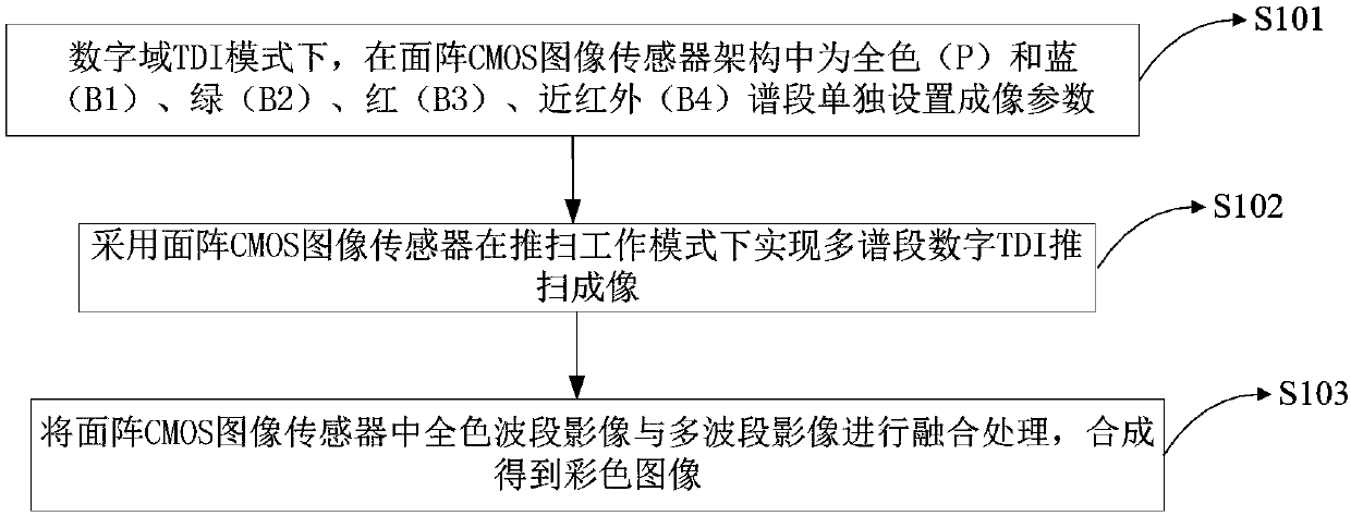
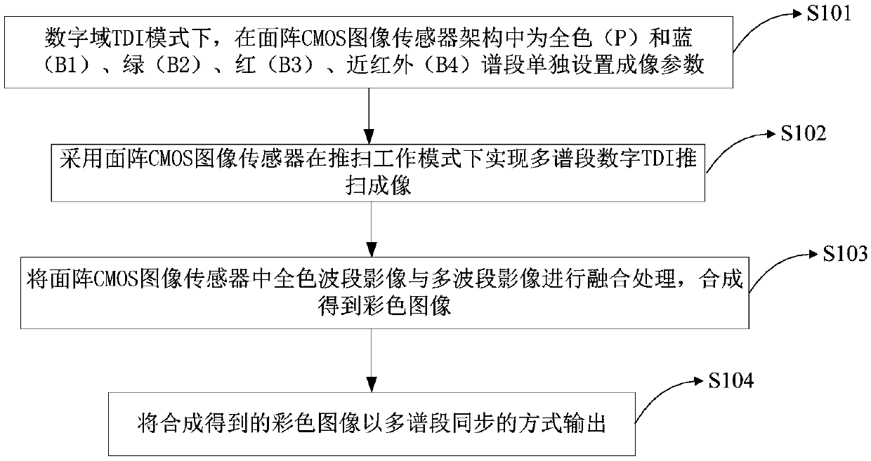
[0034] According to an embodiment of the present invention, a multi-spectral TDI imaging method is provided, see figure 1 , including the following steps:

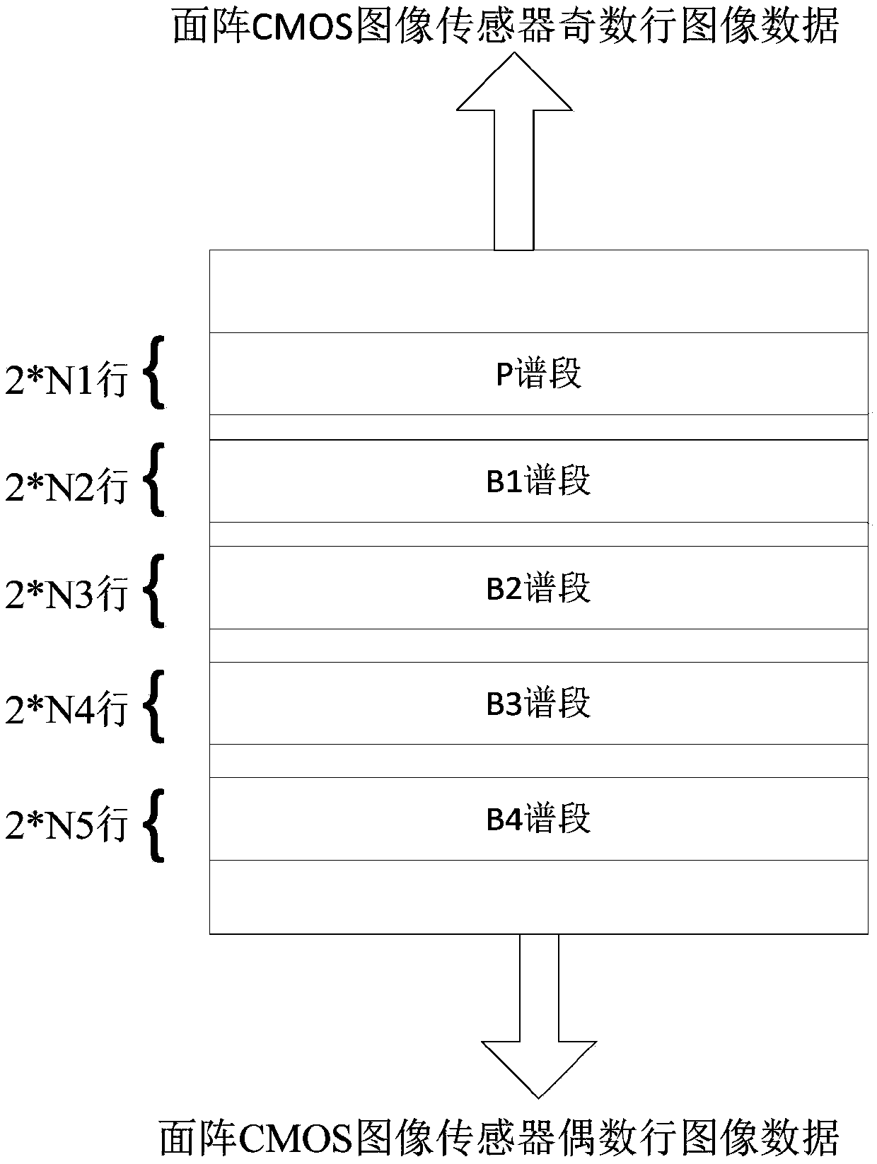
[0035] Step S101: In digital domain TDI mode, separately set imaging parameters for panchromatic (P) and blue (B1), green (B2), red (B3), and near-infrared (B4) spectral bands in the area array CMOS image sensor architecture ;

[0036] Step S102: using an area array CMOS image sensor to realize multi-spectral digital TDI pushbroom imaging in the pushbroom working mode;

[0037] Step S103: Perform fusion processing on the panchromatic band image and the multi-band image in the area array CMOS image sensor to synthesize a color image.

[0038] The multi-spectral TDI imaging method in the embodiment of the present invention uses an area array CMOS image sensor to realize multi-spectral digital TDI push-broom imaging in the push-broom working mode, and performs panchromatic band images and multi-band images in the area array...

Embodiment 2

[0048] According to another embodiment of the present invention, a multispectral TDI imaging device is provided, see Figure 4 ,include:

[0049] The parameter setting unit 10 is used for panchromatic (P) and blue (B1), green (B2), red (B3), near-infrared (B4) spectra in the area array CMOS image sensor architecture in the digital domain TDI mode Set the imaging parameters separately for each segment;

[0050] A push-broom imaging unit 20, configured to use an area array CMOS image sensor to realize multi-spectral digital TDI push-broom imaging in a push-broom working mode;

[0051] The fusion processing unit 30 is configured to perform fusion processing on the panchromatic band image and the multi-band image in the area array CMOS image sensor to synthesize a color image.

[0052] The multi-spectral TDI imaging device in the embodiment of the present invention uses an area array CMOS image sensor to realize multi-spectral digital TDI push-broom imaging in the push-broom wor...


PUM


Abstract

The invention relates to the field of photodetection imaging, and particularly to a multispectral TDI (Time Delayed and Integration) imaging method and device. According to the method and device, imaging parameters are separately set for full-color (P) and blue (B1), green (B2), red (B3) and near-infrared (B4) spectrum segments in an area array CMOS image sensor architecture in a digital domain TDI mode, area array CMOS image sensors are used to realize multi-spectrum-segment digital TDI push-broom imaging in a push-broom work mode, a full-color waveband image and a multi-waveband image in thearea array CMOS image sensors are fused, a color image is obtained by synthesis, the full-color remote sensing image and the multi-waveband image are fused to obtain the image which has high resolution of the full-color image and also has color information of the multi-waveband images, and imaging accuracy is high.

Description

technical field [0001] The invention relates to the field of photoelectric detection imaging, in particular to a multispectral TDI imaging method and device. Background technique [0002] TDI (Time Delayed and Integration) technology can greatly improve the sensitivity and signal-to-noise ratio of the imaging system by accumulating multiple exposures of the same target. Space remote sensing field. Especially as people's requirements for remote sensing image resolution are getting higher and higher, TDI imaging technology is widely used in the field of high-resolution space remote sensing. [0003] At present, TDI CCDs are generally used as detectors in the field of high-resolution space remote sensing. TDI CCD is an ideal device to realize TDI, and its time delay integration process occurs in the charge domain. Driven by strict vertical transfer timing and horizontal transfer timing, charges are transferred, integrated, and output between the vertical shift register and t...

Claims


Application Information

Patent Timeline
IPC IPC(8): H04N5/374H04N5/372H04N5/265H04N9/04H04N9/64H04N9/44
CPCH04N5/265H04N9/44H04N9/64H04N25/71H04N25/76H04N23/10
Inventor 薛旭成韩诚山胡长虹黄良李洪法
Owner CHANGCHUN INST OF OPTICS FINE MECHANICS & PHYSICS CHINESE ACAD OF SCI
Learn More