Liquid crystal display device

A technology of liquid crystal display device and liquid crystal display panel, which is applied in static indicators, optics, instruments, etc., can solve the problems of affecting the screen ratio, difficult to apply LCD display, and inconvenient for users to use.

Active Publication Date: 2019-04-19
KUSN INFOVISION OPTOELECTRONICS
View PDF4 Cites 12 Cited by
  • Summary
  • Abstract
  • Description
  • Claims
  • Application Information

AI Technical Summary

Problems solved by technology

At present, it is usually necessary to set up a separate fingerprint recognition area for fingerprint recognition. However, with the popularity of full screens, the separate fingerprint recognition area has become an important factor affecting the screen-to-body ratio.
For this reason, most of the current fingerprint recognition can only be moved to the side or back of the electronic device, which brings great inconvenience to the user.
[0004] With the advancement of science and technology, due to the thinner OLED display, in recent years, the under-screen fingerprint recognition technology applicable to OLED displays has gradually emerged to realize full-screen fingerprint recognition. Passively emits light, so the technology is difficult to apply to LCD displays

Method used


Image

  • Liquid crystal display device
  • Liquid crystal display device
  • Liquid crystal display device

Examples


no. 1 example

[0032] figure 1 is a schematic cross-sectional structure diagram of a liquid crystal display device according to the first embodiment of the present invention, figure 2 for figure 1 A schematic plan view of the fingerprint identification module of the liquid crystal display device shown, image 3 for figure 1 The schematic diagram of the fingerprint recognition of the liquid crystal display device shown, Figure 4 for figure 1 The schematic diagram of the circuit principle of the liquid crystal display device shown, Figure 5 for figure 1 The schematic diagram of the liquid crystal display device outputting electrical signals when the ambient light intensity is weak is shown, Figure 6a and Figure 6b for figure 1 The schematic diagram of the fingerprint recognition pattern of the liquid crystal display device shown when the ambient light intensity is relatively weak when there is no finger pressing and when there is finger pressing, Figure 7 for figure 1 The schem...

no. 2 example

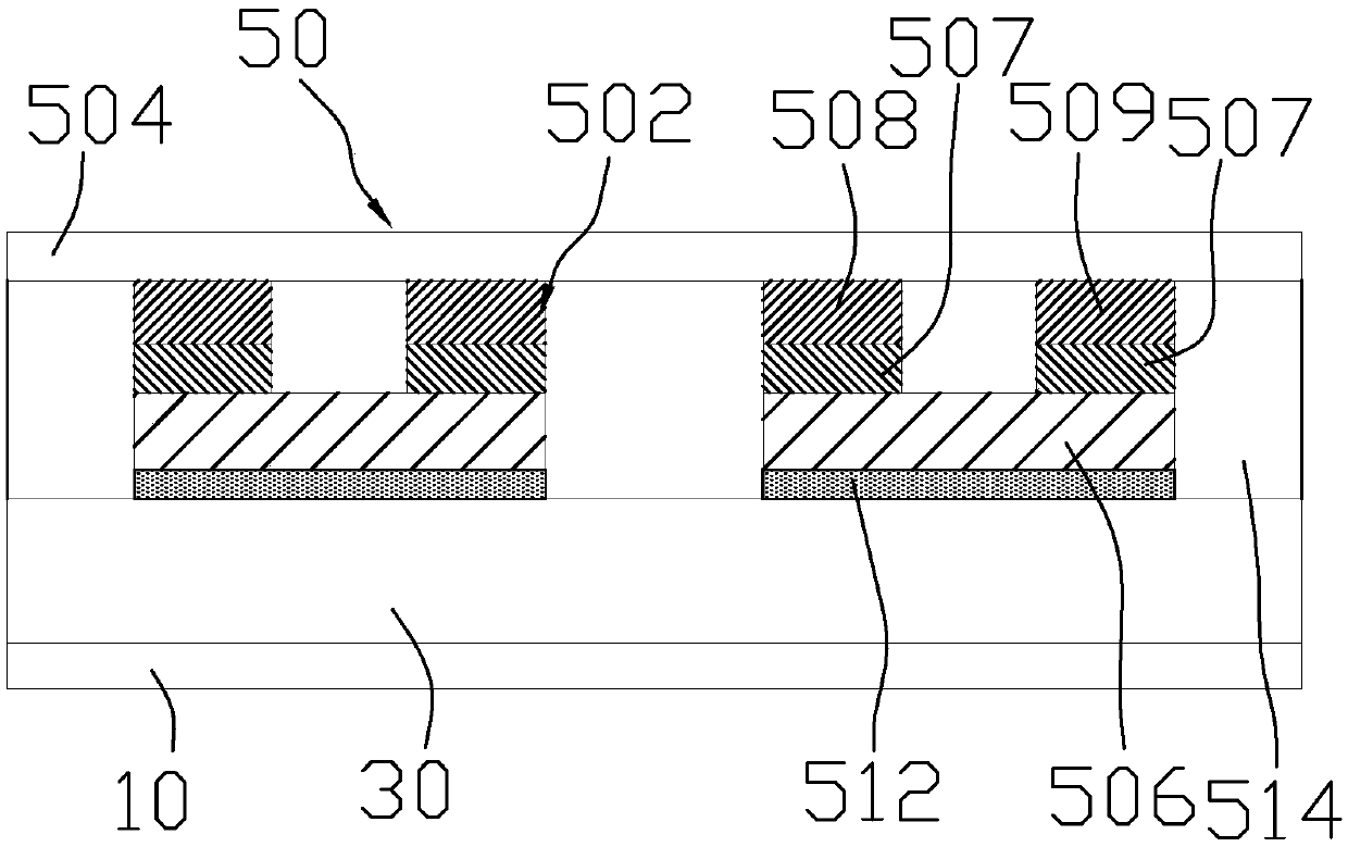
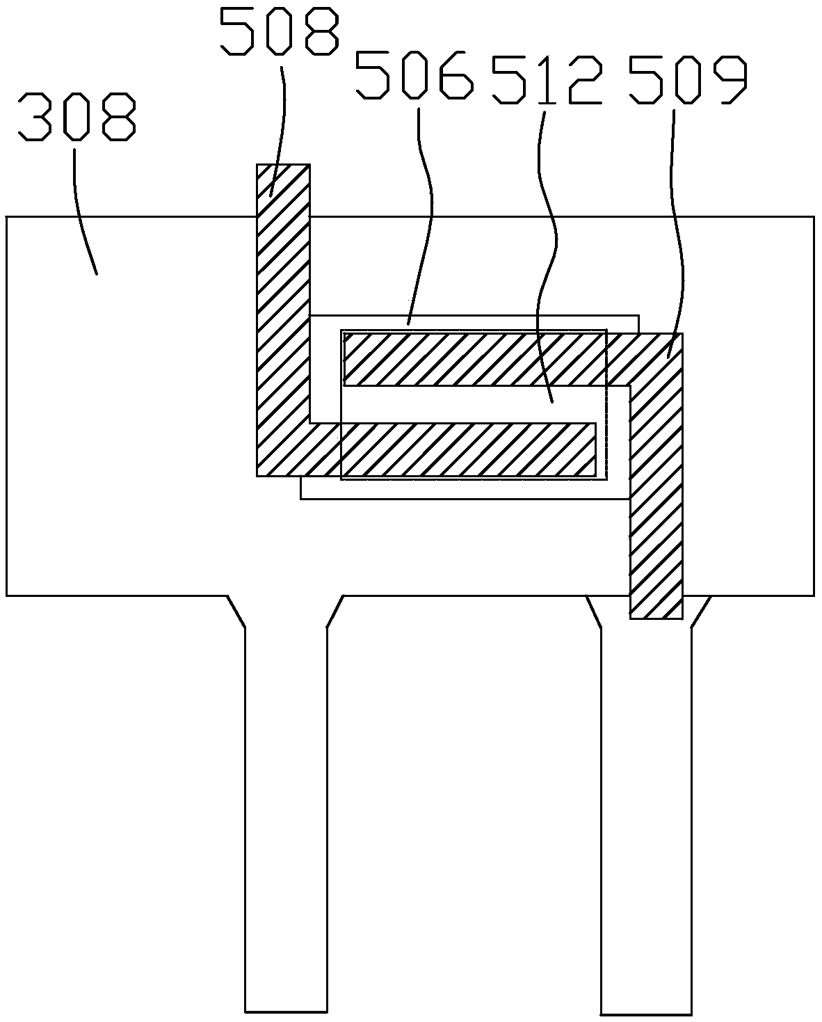
[0045] Figure 10 It is a schematic cross-sectional structure diagram of a liquid crystal display device according to the second embodiment of the present invention, as Figure 10 As shown, the liquid crystal display device of the second embodiment of the present invention is basically similar to the liquid crystal display device of the first embodiment, the difference is that in the liquid crystal display device of the second embodiment, the fingerprint recognition module 502 includes a sensing layer 506, a Region 507, source electrode 508 and drain electrode 509, source electrode 508 and drain electrode 509 are arranged on the side of liquid crystal display panel 30 away from backlight module 10, two diffusion regions 507 are arranged on source electrode 508 and drain electrode 509 respectively, The sensing layer 506 is disposed on the two diffusion regions 507 at the same time. Wherein, the sensing layer 506 is made of amorphous silicon (a-Si) material. Other structures o...


PUM


Abstract

The invention discloses a liquid crystal display device. The liquid crystal display device comprises a backlight module, a liquid crystal display panel and a fingerprint recognition layer, the backlight module, the liquid crystal display panel and the fingerprint recognition layer are stacked in sequence, the liquid crystal display panel is arranged between the backlight module and the fingerprintrecognition layer, the fingerprint recognition layer comprises multiple fingerprint recognition modules and a substrate, the fingerprint recognition modules are arranged at intervals, each fingerprint recognition module comprises a sensing layer, a source electrode and a drain electrode, the source electrodes and the drain electrodes are spaced, the substrate covers the source electrodes and thedrain electrodes, and the sensing layers are made of amorphous silicon materials and used for sensing light intensity and generating leakage current. According to the liquid crystal display device, the fingerprint recognition layer can be arranged in any area of the liquid crystal display device, thus fingerprint recognition is achieved in all areas of the liquid crystal display device, normal display is not influenced, arrangement of an individual recognition area is not needed, the device is suitable for fingerprint recognition of a whole-plane screen, and the screen occupying ratio of a front panel of the liquid crystal display device is also effectively increased; the sensing layers have high sensing sensitivity to light intensity, the fingerprint recognition speed is high, and the fingerprint recognition precision is also high.

Description

technical field [0001] The invention relates to the technical field of liquid crystal display, in particular to a liquid crystal display device. Background technique [0002] Liquid crystal display devices have the advantages of good image quality, small size, light weight, low driving voltage, low power consumption, no radiation, and relatively low manufacturing costs, and occupy a dominant position in the field of flat panel displays. [0003] In order to achieve greater convenience in human-computer interaction, operations such as unlocking electronic devices are usually performed by fingerprint recognition. At present, it is usually necessary to set a separate fingerprint recognition area for fingerprint recognition. However, with the popularity of full screens, the separate fingerprint recognition area has become an important factor affecting the screen-to-body ratio. For this reason, most fingerprint identifications can only be moved to the side or back of the electro...

Claims


Application Information

Patent Timeline
Patent Type & Authority Applications(China)
IPC IPC(8): G02F1/1333G02F1/1335G02F1/13357G09G3/34G06K9/00
CPCG02F1/1333G02F1/13338G02F1/133512G02F1/1336G09G3/342G06V40/1318
Inventor 贾本超赵中满
Owner KUSN INFOVISION OPTOELECTRONICS
Why Eureka
Try Eureka