Method for improving precision of positioning defects on chip to graphic layer

A graphics layer and accuracy technology, applied in the field of improving the positioning accuracy of defects on the optical sheet to the graphics layer, can solve the problems of inaccurate positioning, the influence of subsequent image formation, and the inability to accurately judge small-sized defects, so as to improve the yield, The effect of reducing the number and speeding up the R&D process

Active Publication Date: 2019-04-19
SHANGHAI HUALI INTEGRATED CIRCUTE MFG CO LTD
View PDF6 Cites 1 Cited by
  • Summary
  • Abstract
  • Description
  • Claims
  • Application Information

AI Technical Summary

Problems solved by technology

When observing defects by electron beam scanning, the positioning is carried out according to the cross marks in the silicon wafer. There is a certain displacement deviation between the two positioning systems, so the defects on the optical wafers are inaccurately positioned to the subsequent fixed-point electron beam scanning observation defects on silicon wafers with pattern layers. The problem of small size defects cannot be accurately judged, which will affect the subsequent graphics.
Evaluation of Factors That Seriously Affect Defects on Wafer Yield

Method used


Image

  • Method for improving precision of positioning defects on chip to graphic layer
  • Method for improving precision of positioning defects on chip to graphic layer
  • Method for improving precision of positioning defects on chip to graphic layer

Examples


Embodiment Construction

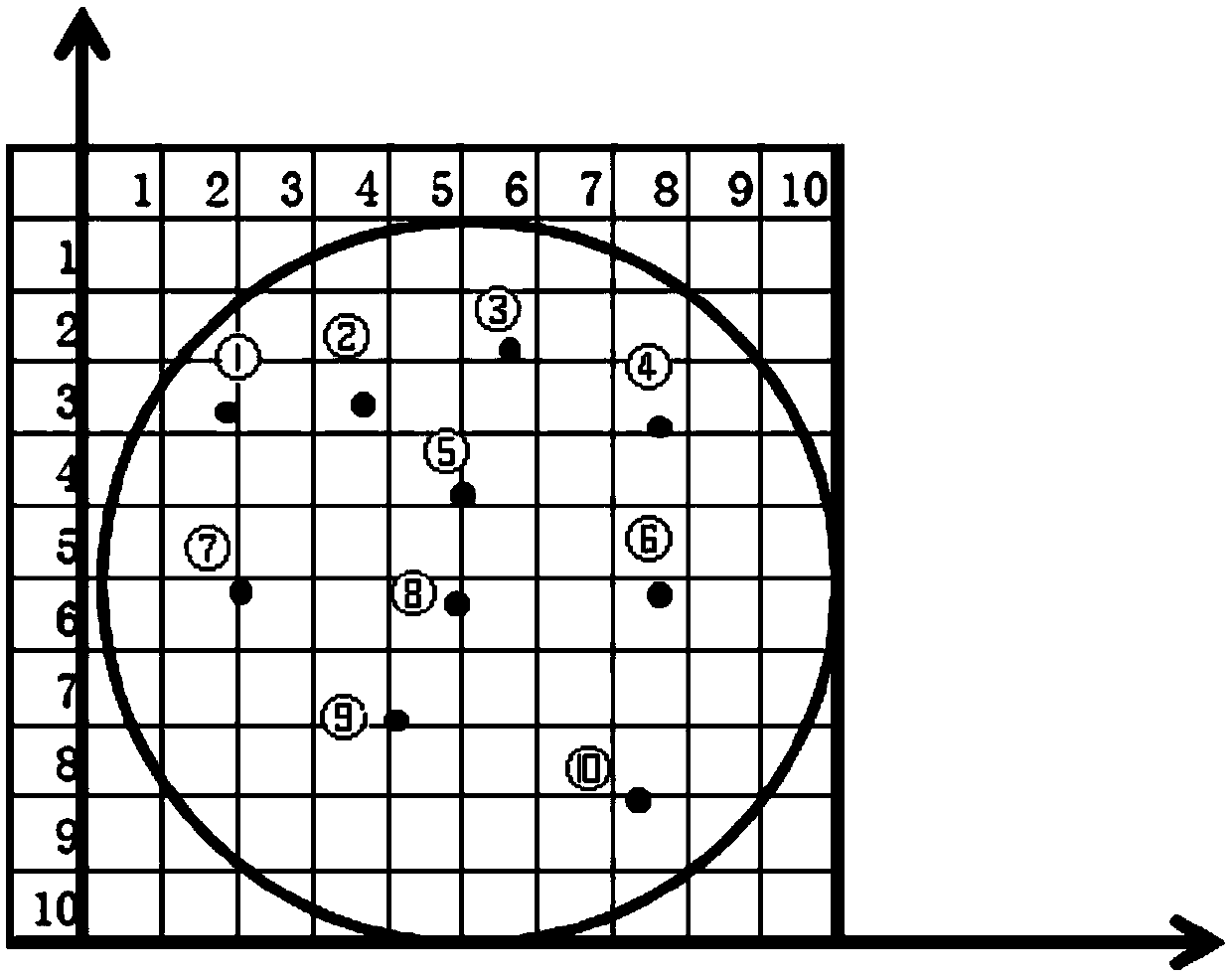
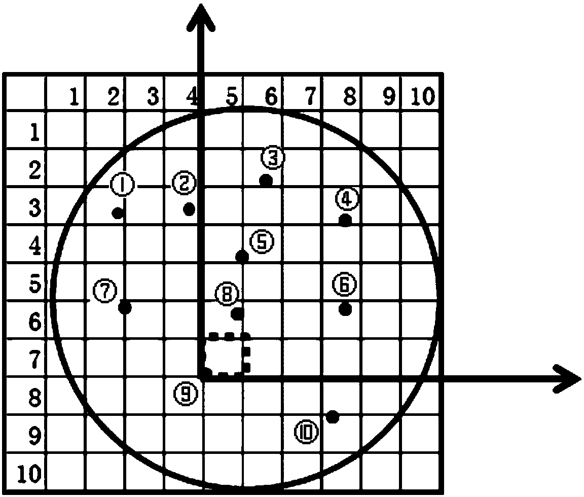
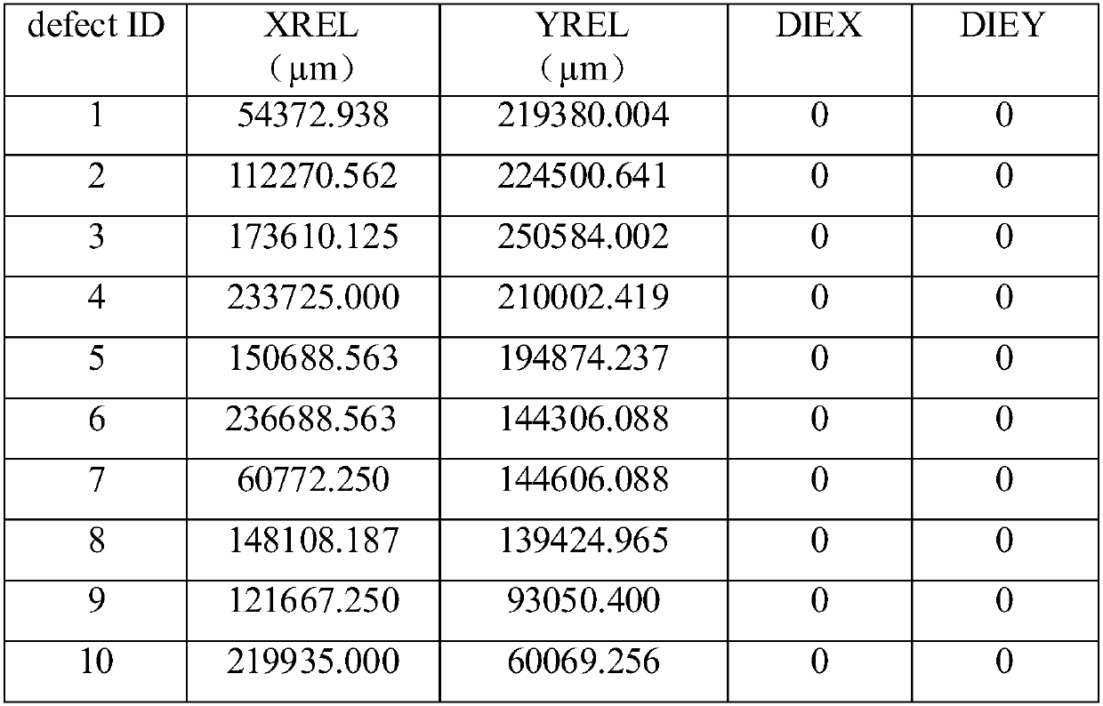
[0010] The method for improving the positioning accuracy of defects on the optical sheet to the graphics layer is based on the principle of adding the smallest repeated complete unit information to the silicon wafer according to the results of electron beam scanning to observe the defects, and then according to the smallest repeated complete unit original complete unit The setting of the origin re-gives each defect a coordinate, so as to improve the positioning of the subsequent silicon wafer with a pattern layer. The specific method is as follows:

[0011] After the bare wafer is scanned in the bright field or dark field, since there is no pattern on the surface of the silicon wafer, the entire silicon wafer is regarded as a minimum repeated complete unit, and a coordinate position is defined for each defect, such as figure 1 As shown in Table 1, when electron beam scanning is used to observe defects, silicon wafers are aligned according to the notch and crystal edge used for...


PUM


Abstract

The invention discloses a method for improving precision of positioning defects on chip to a graphic layer. The method comprises the steps of: adding minimal repeated complete unit information to a silicon wafer according to a defect result observed by electron beam scanning; and reassigning coordinates to each defect according to the setting of an original point of an original complete unit of the minimal repeated complete unit, so as to improve the positioning of subsequent silicon wafer with the graphic layer. The method can automatically add the minimal repeated complete unit information,and improve the precision of positioning the defects in the bare wafer to later wafers with graphic layers.

Description

technical field [0001] The invention relates to the field of semiconductor integrated circuits, in particular to a method for improving the positioning accuracy of a defect on an optical sheet to a graphic layer. Background technique [0002] In the production process of large-scale integrated circuit wafers, it is necessary to detect defects in different processes in a timely manner. The common method is to scan the bright field and dark field. There is no graphics, and the entire silicon wafer is regarded as a complete unit with the smallest repetition. When the electron beam scans to observe the defects, the silicon wafer is aligned according to the notch and the crystal edge used for marking on the silicon wafer, and the silicon wafer wafer with the normal pattern layer has the smallest repeated complete unit information. When observing defects by electron beam scanning, the positioning is carried out according to the cross marks in the silicon wafer. There is a certain...

Claims


Application Information

Patent Timeline
Patent Type & Authority Applications(China)
IPC IPC(8): H01L21/66
CPCH01L22/12H01L22/20
Inventor 沈萍郭浩倪祺梁
Owner SHANGHAI HUALI INTEGRATED CIRCUTE MFG CO LTD
Why Eureka
Try Eureka