Wafer defect analysis system

A defect analysis, wafer technology, applied in electrical components, semiconductor/solid-state device manufacturing, semiconductor/solid-state device testing/measurement, etc., can solve problems affecting wafers, wafers are not easy to find, error-prone, etc., to facilitate troubleshooting , saving manpower and time

Active Publication Date: 2014-01-22
SHANGHAI HUALI MICROELECTRONICS CORP
View PDF3 Cites 6 Cited by
  • Summary
  • Abstract
  • Description
  • Claims
  • Application Information

AI Technical Summary

Problems solved by technology

These process deviation machines are often not easy to be found on the defective wafers generated in the early stage. After a period of time, they will continue to affect a large number of wafers, and will not be discovered until the number of defects and the scope of influence gradually increase.
The existing technology is usually to send engineers to inspect all the scanned wafers at regular intervals to find out the possible existence of specific defects in the same position. Due to manual judgment and manual operation, one is time-consuming and labor-intensive, and the other is Error-prone

Method used


Image

  • Wafer defect analysis system

Examples


Embodiment Construction

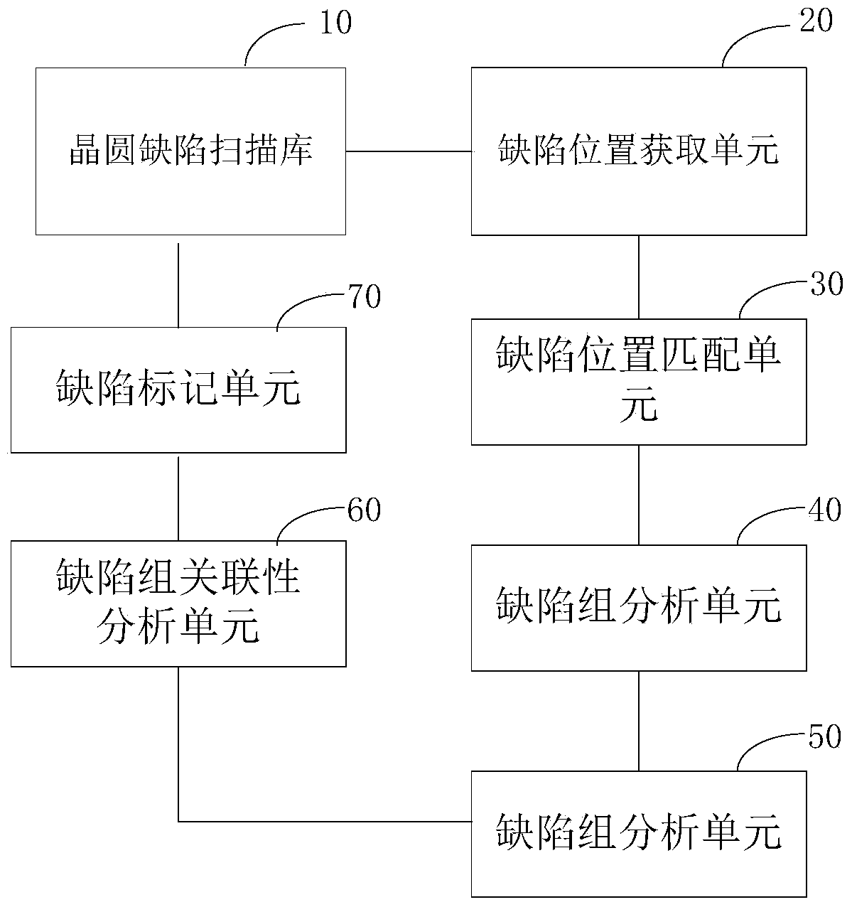
[0020] The problem to be solved by the present invention is to provide a wafer defect analysis system, which can analyze the scanning image of wafer defects, and highlight relevant defects, so as to facilitate timely investigation of the same defect at a specific position of the wafer.

[0021] In order to solve the above problems, a wafer defect analysis system of the present invention comprises:

[0022] The wafer defect scanning library is used to store the defect scanning diagrams of the wafers scanned by the wafer scanning machine within a set time, and the wafers include at least two batches of wafers;

[0023] A defect position acquisition unit, configured to obtain position information of defects based on the defect scanning diagram, and sort the position information, the position information includes an abscissa and a ordinate;

[0024] a defect position matching unit, configured to match the position information of a defect in the defect scan map of a wafer with the ...


PUM


Abstract

The invention provides a wafer defect analysis system. The wafer defect analysis system comprises a wafer defect scanning library, a defect position obtaining unit, a defect position matching unit, a defect set analysis unit, a defect set correlation analysis unit and a defect marking unit, wherein the wafer defect scanning library is used for storing defect scanning graphs of a wafer scanned by a wafer scanning drilling crew in pre-set time; the defect position obtaining unit for sorting position information; the defect position matching unit is used for matching the position information of one defect in the defect scanning graph of one wafer with the position information of one defect in the defect scanning graph of the other wafer, and marking a matched set; the defect set analysis unit is used for obtaining position information of a defect set; the defect set correlation analysis unit is used for carrying out a correlation analysis on the position information of the defect set between the two wafers; and the defect marking unit is used for displaying the defects with the correlation in the defect scanning graphs by highlight. The wafer defect analysis system can be used for analyzing the defect scanning graphs and can mark the defects with the correlation by the highlight so that in-time troubleshooting of the same defect condition of the specific positions of the wafer is convenient to carry out and the manpower and the time are saved.

Description

technical field [0001] The invention relates to the technical field of semiconductor technology manufacturing, in particular to a wafer defect analysis system. Background technique [0002] At present, due to the short process time of some process machines in the semiconductor manufacturing industry, once there is a process deviation due to machine abnormalities, it is easy to cause a large number of wafers to have defects at the same specific position, that is, the continuous passing of this process machine Wafers will all have defects at the same location. For example, the single-point out-of-focus defect of the lithography machine, the chromatic aberration defect caused by the deviation of the wafer support column, etc. These process deviation machines are often not easy to be found on the defective wafers generated in the early stage. After a period of time, they will continue to affect a large number of wafers, and will not be discovered until the number of defects and...

Claims


Application Information

Patent Timeline
IPC IPC(8): H01L21/66H01L21/67
CPCH01L22/12H01L22/24
Inventor 郭贤权许向辉陈超
Owner SHANGHAI HUALI MICROELECTRONICS CORP
Why Eureka
Try Eureka