Chip to be filmed and its processing technology

A processing technology and chip technology, applied in the direction of semiconductor devices, electrical components, circuits, etc., can solve the problems of high application failure rate and high edge collapse rate

Active Publication Date: 2020-07-07
JILIN SINO MICROELECTRONICS CO LTD
View PDF2 Cites 0 Cited by
  • Summary
  • Abstract
  • Description
  • Claims
  • Application Information

AI Technical Summary

Problems solved by technology

[0004] The first purpose of the present invention is to provide a treatment process for chips to be film-mounted, which solves the technical problems of high chipping rate after scribing, slicing through silicon powder and high application failure rate after packaging in the traditional process.

Method used


Image

  • Chip to be filmed and its processing technology
  • Chip to be filmed and its processing technology
  • Chip to be filmed and its processing technology

Examples


Embodiment 1

[0071] This embodiment provides a chip to be film-mounted, and its processing technology includes the following steps:

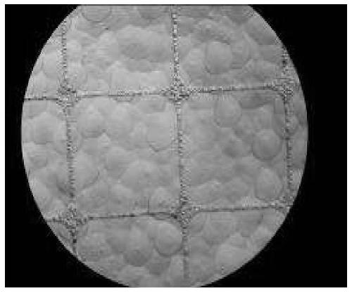
[0072] (a) first chip is carried out acid solution chemical corrosion, and wherein acid solution is the mixed solution of hydrofluoric acid solution and nitric acid solution, and the volume ratio of hydrofluoric acid solution (50wt%) and nitric acid solution (570wt%) is 1:5, Then select the chip after double-sided chemical etching to ensure that the etched lattice width is controlled at 300 μm and evenly distributed, and there are silicon oxide layers on the upper and lower surfaces of the chip;

[0073] (b) the lower surface of the chip is divided into a plurality of first sub-regions by photolithography, the first sub-regions include the first middle region and the first edge region, and the silicon oxide layer in the first middle region is removed, Then boron doping, aluminum doping and photolithography are performed on the first middle region to remove t...

Embodiment 2

[0076] This embodiment provides a chip to be film-mounted. The difference between the processing technology of this embodiment and Embodiment 1 is that the etching lattice width is 100 μm.

Embodiment 3

[0078] This embodiment provides a chip to be film-mounted. The difference between the processing technology of this embodiment and Embodiment 1 is that the etching lattice width is 500 μm.


PUM

PropertyMeasurementUnit
depthaaaaaaaaaa

Abstract

The present invention provides a chip to be coated and a processing process thereof, and relates to the technical field of chip manufacturing. The process for processing the chip to be coated includesthe following steps: a chip is provided, the chip includes an upper surface and a lower surface disposed opposite to each other, the lower surface of the chip is provided with a silicon oxide layer,the lower surface of the chip is divided into a plurality of first sub-regions, and each of the first sub-regions includes a first intermediate region and a first edge region, a silicon oxide layer ofthe first intermediate region is removed, the first intermediate region is subjected to boron doping, aluminum doping, and aluminum layer removal, to form a first sub-region with a recessed first intermediate region, the first intermediate region is corroded, the corrosion depth is 3-8Mum, and the chip to be coated is obtained. The technical problems that a conventional process has high chippingrate after dicing, siliconized powder is scratched and the application failure rate after packaging is high are solved. The process for processing the chip to be coated is simple and convenient to operate, a device is simple, and an application prospect is wide.

Description

technical field [0001] The invention relates to the technical field of chip manufacturing, in particular to a chip to be laminated and a processing technology thereof. Background technique [0002] In the "split" step in the semiconductor chip manufacturing process, the wafer needs to be cut into individual chips in the direction of the scribing line for packaging. Chip splitting is generally carried out by grinding wheel dicing machine, that is, the back of the wafer is glued on the cutting film, and the wafer is cut and split by a high-speed rotating dicing knife. However, in order to reduce the cost of double-sided chips, most manufacturers now use substrate The chip chooses double-sided chemical etching instead of double-sided polishing, and at the same time replaces the boron-to-diffusion process with the aluminum expansion process, but the new problem brought about by this process is that the back of the chip is uneven and the roughness is extremely poor. The roughnes...

Claims


Application Information

Patent Timeline
Patent Type & Authority Patents(China)
IPC IPC(8): H01L21/78H01L21/683
CPCH01L21/6835H01L21/78H01L2221/68327
Inventor 车振华耿智蔷汪金磊李超
Owner JILIN SINO MICROELECTRONICS CO LTD
Why Eureka
Try Eureka