Method for monitoring edge defect of wafer
A defect and crystal edge technology, which is applied in the field of crystal edge defect monitoring, can solve the problems that the monitoring method cannot be found in the first time, timeliness delay, and online monitoring cannot be performed, so as to improve test efficiency, improve quality, and reduce test cost effect
- Summary
- Abstract
- Description
- Claims
- Application Information
AI Technical Summary
Problems solved by technology
Method used
Image

Examples
Embodiment Construction
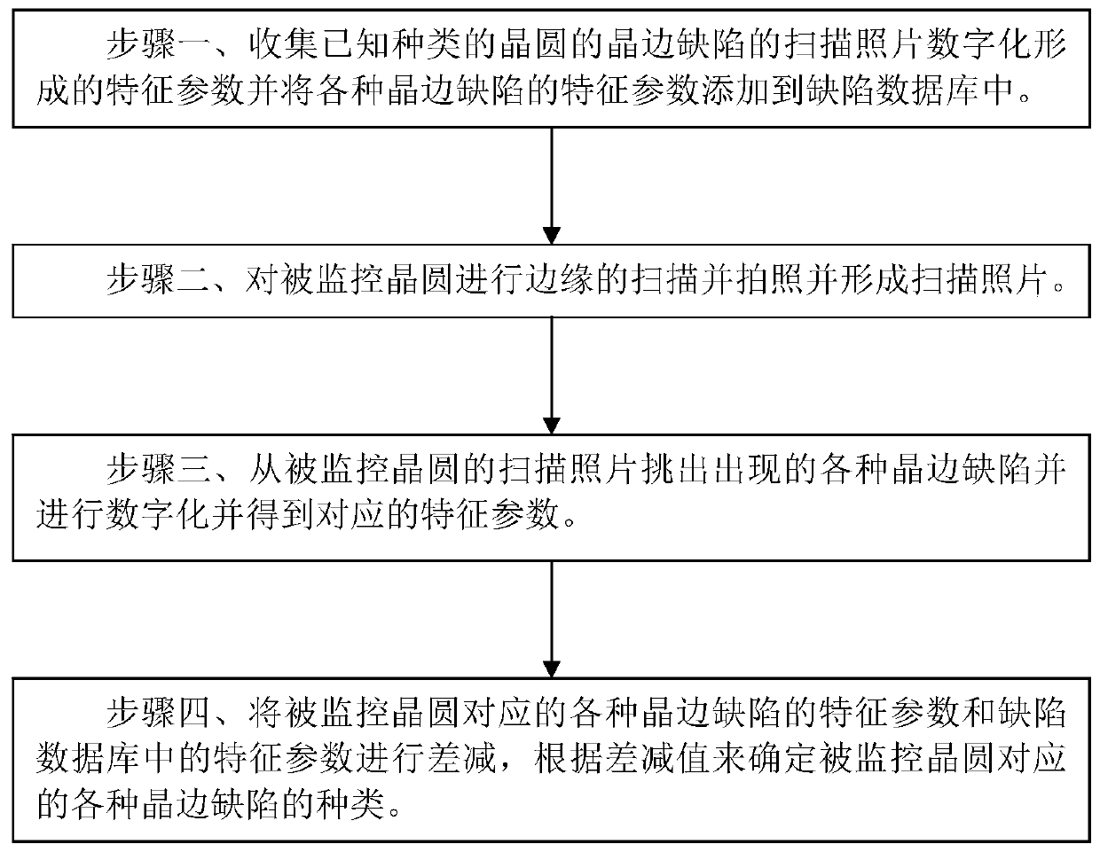
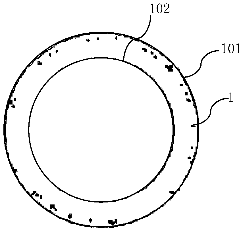
[0033] Such as figure 1 As shown, it is a flow chart of the method for monitoring the edge defect 1 of the wafer 101 according to the embodiment of the present invention. The method for monitoring the edge defect 1 of the wafer 101 according to the embodiment of the present invention includes the following steps:
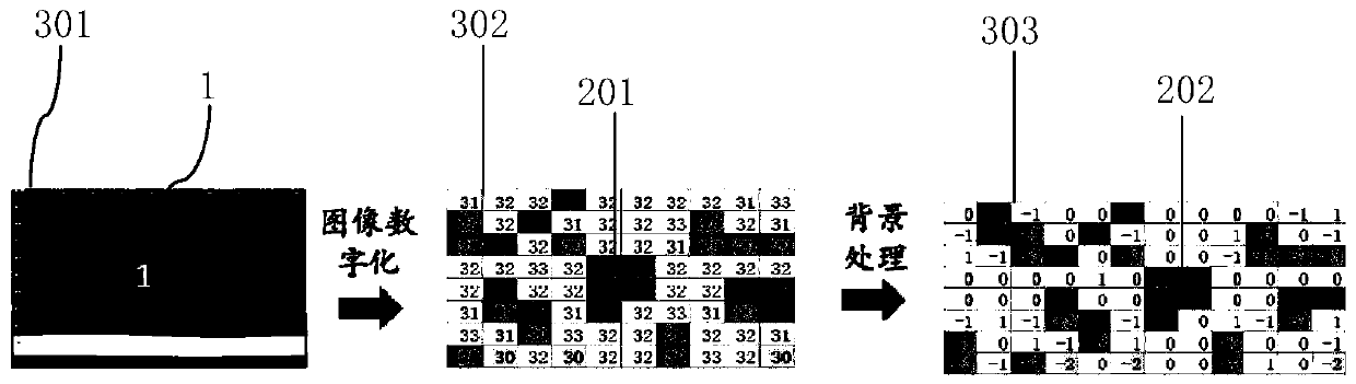
[0034] Step 1, collect the characteristic parameters of the crystal edge defects 1 of known types of wafers 101, the characteristic parameters are scanned and photographed by scanning and photographing the crystal edge defects 1 of the corresponding edge of the wafer 101 and all the parameters in the scanned photos are The photographs of the crystal edge defects 1 are digitally formed, and the characteristic parameters of all known types of the crystal edge defects 1 are added to the defect database.
[0035] Preferably, a defect inspection machine is used to scan and photograph corresponding edge defects 1 on the edge of the wafer 101 . When collecting the charact...
PUM
 Abstract
Description
Claims
Application Information
 - R&D
- Intellectual Property
- Life Sciences
- Materials
- Tech Scout
- Unparalleled Data Quality
- Higher Quality Content
- 60% Fewer Hallucinations
Browse by: Latest US Patents, China's latest patents, Technical Efficacy Thesaurus, Application Domain, Technology Topic, Popular Technical Reports.
© 2025 PatSnap. All rights reserved.Legal|Privacy policy|Modern Slavery Act Transparency Statement|Sitemap|About US| Contact US: help@patsnap.com