Binding method of display device and display substrate

A technology for display substrates and display devices, which is applied to the assembly of printed circuits, optics, instruments, etc. with electrical components, and can solve the problems of complex binding process and high cost of display substrates

Active Publication Date: 2019-05-10
BOE TECH GRP CO LTD
View PDF8 Cites 16 Cited by
  • Summary
  • Abstract
  • Description
  • Claims
  • Application Information

AI Technical Summary

Problems solved by technology

It can solve the complicated and costly problem of binding the display

Method used


Image

  • Binding method of display device and display substrate
  • Binding method of display device and display substrate
  • Binding method of display device and display substrate

Examples


Embodiment Construction

[0039] In order to make the objectives, technical solutions, and advantages of the present invention clearer, the embodiments of the present invention will be described in further detail below in conjunction with the accompanying drawings.

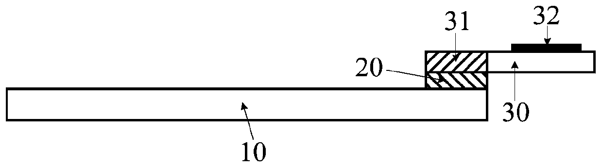
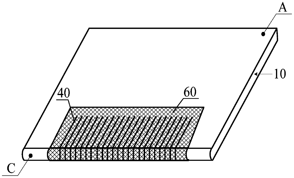
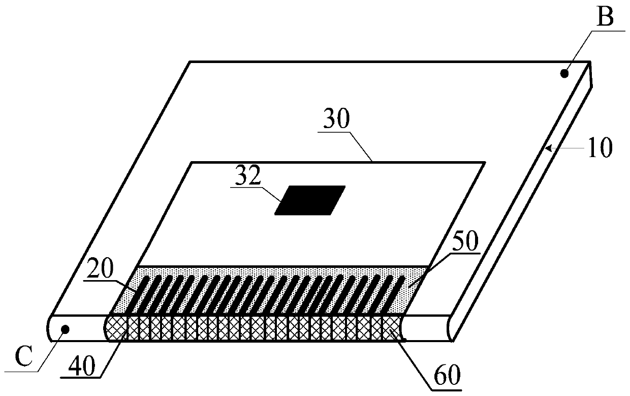
[0040] The embodiment of the present invention provides a display device. The display device may generally be any product or component with display function, such as electronic paper, mobile phone, tablet computer, television, monitor, notebook computer, digital photo frame, navigator, etc. Such as figure 1 As shown, figure 1 It is a schematic structural diagram of a display device provided by an embodiment of the present invention. The display device may include:

[0041] The display substrate 10, the binding structure 20 and the circuit board 30 are shown.

[0042] The display substrate 10 is provided with signal lines ( figure 1 (Not shown in the figure), the circuit board 30 includes a first conductive structure 31 and a display driving chip...


PUM


Abstract

The invention discloses a binding method of a display device and a display substrate, and belongs to the field of display technology. The display device includes a display substrate, a binding structure and a circuit board, wherein the binding structure is arranged on the display substrate, is made of a conductive tape, and has a certain stickiness; and the binding structure can be directly bondedto the first conductive structure of the circuit board. The electrical connection between the binding structure and the first conductive structure can be realized without using ACF to bond the binding structure to the first conductive structure; the process of binding the display substrate is effectively simplified; and the cost is lowered.

Description

Technical field [0001] The present invention relates to the field of display technology, in particular to a display device and a method for binding a display substrate. Background technique [0002] With the development of the display technology field, various products with display functions appear in daily life, such as mobile phones, tablets, televisions, laptops, digital photo frames, and navigators. All of these products need to be equipped with displays without exception. Substrate. [0003] For example, the display substrate may be: an array substrate in a liquid crystal display panel, an organic light emitting diode (English: Organic Light Emitting Diode, abbreviation: OLED) display substrate, or a micro light emitting diode (English: MicroLight Emitting Diode, abbreviation: Micro LED) display Substrate etc. [0004] In order to enable the display substrate to perform normal display, it is necessary to ensure that the internal signal traces are electrically connected to the ...

Claims


Application Information

Patent Timeline
IPC IPC(8): G02F1/1345H05K3/32
Inventor 王莉莉刘超汪楚航崔强伟孟柯
Owner BOE TECH GRP CO LTD
Why Eureka
Try Eureka