
Probe card

A technology of probe cards and substrates, applied in the field of probe cards, can solve problems such as inability to further improve, plate burst, drill bit breakage of drilling holes, etc., achieve decentralized production risks, reduce production costs, and facilitate mass production of modularization Effect

Inactive Publication Date: 2019-05-21
MICROELECTRONICS TECH INC
View PDF9 Cites 0 Cited by
  • Summary
  • Abstract
  • Description
  • Claims
  • Application Information

AI Technical Summary

Problems solved by technology

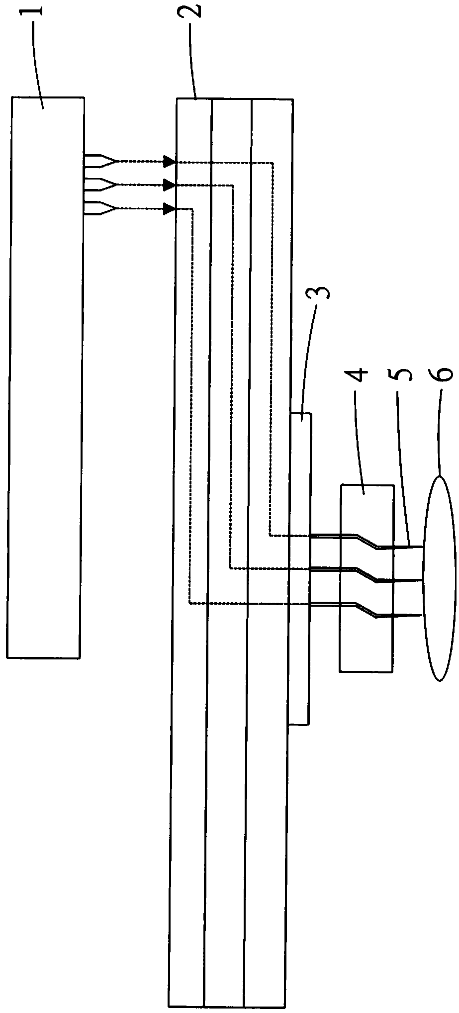
Among them, the traditional structure of the circuit board 2 mostly uses a lamination process to press multiple substrates (such as glass fiber boards, etc.) into one body, and there must be no gaps between the substrates, otherwise the gaps will easily accumulate moisture and air residues. , it is easy to produce popcorn effect (Popcorn Effect) when using it, and there is a risk of bursting
[0003] In addition, for the circuit board 2 traditionally manufactured by lamination process, as the number of laminated substrates increases, the tolerance of its lamination alignment will also increase. In addition, if mechanical drilling (such as back drilling) is required after lamination ), it is easy to have the problem that the friction force is too high due to the high number of stacked layers and the increase of the total thickness, so that the drilling bit is prone to breakage. Therefore, the depth ratio of the circuit board of the general traditional lamination process ( plate thickness / drilling hole diameter) probably has its limitations and cannot be further improved
Furthermore, the circuit board without the back-drilling process will have multiple through-hole stubs (Via Stub), which is prone to produce the Via Stub Effect and easily increase the amount of reflection during signal transmission.

Method used


Image

  • Probe card
  • Probe card
  • Probe card

Examples


Embodiment Construction

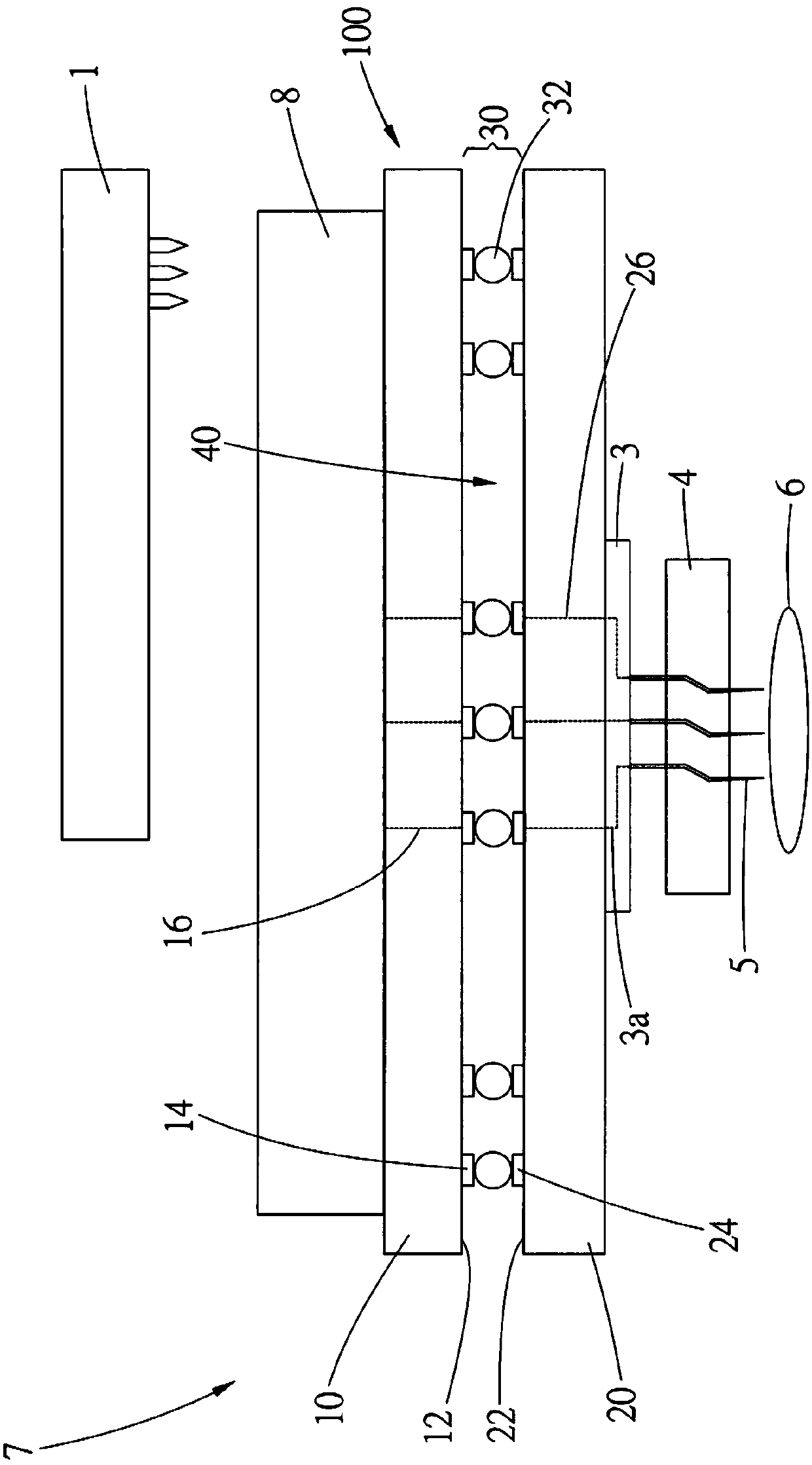
[0059] In order to illustrate the present invention more clearly, embodiments are given and detailed descriptions are as follows in conjunction with the accompanying drawings. Please refer to figure 2Shown is a probe card 7 according to a first embodiment of the present invention, which is used to transmit a signal of a tester 1 to an electronic object 6 to be tested, and includes a modular circuit board 100 and a plurality of probes 5 . The modular circuit board 100 includes a first substrate 10 , a second substrate 20 and an interposer 30 .

[0060] The first substrate 10 has a first surface 12 on which a plurality of first conductive pads 14 are arranged, and in addition, a plurality of first conductive circuits 16 are arranged in the first substrate 10 (Fig. Only some lines are shown in the formula), one end of these first conductive lines 16 is connected to the transmission interface (not shown) on the upper surface (the surface opposite to the first surface 12), and th...


PUM


Abstract

A probe card for transmitting a signal of a detector to an electronic object to be tested, comprising: a modular circuit board comprising a first substrate, a first conductive line electrically connected, and a plurality of a first conductive pad, one end of the first conductive line is electrically connected to the detecting; a second substrate has a gap between the first substrate, and the second substrate is provided with a second conductive line electrically connected and a plurality of a conductive pad; an interposer disposed in the gap between the first substrate and the second substrate, the interposer comprising a plurality of electrical conductors, the electrical conductors being electrically connected to the first conductive pads And the second conductive pads; the plurality of probes, one end is electrically connected to the second conductive line, and the other end is in contact with the electronic object to be tested.

Description

technical field [0001] The present invention relates to a probe card; in particular, it refers to a probe card structure in which the circuit board structure of the probe card can be stacked in high layers, and has the advantages of high aspect ratio, short through-holes of signal paths, and the like. Background technique [0002] Please refer to figure 1 As shown, the structure of a general probe test system generally includes a detector 1, a circuit board 2, a carrier board 3, a pin seat 4 and a plurality of probes 5, and the detector 1 is used to pass through a circuit board (such as a PCB) ) 2, the carrier board 3 (such as MLO, MLC) and the probe card frameworks such as these probes 5 carry out signal detection and electrical analysis to an electronic object 6 to be tested, wherein the carrier board 3 is mainly used for the circuit board 2 The lines are space-transformed to match the smaller-pitched probes. Among them, the traditional structure of the circuit board 2 m...

Claims


Application Information

Patent Timeline
Patent Type & Authority Applications(China)
IPC IPC(8): G01R1/04G01R31/00
Inventor 顾伟正赖俊良何志浩
Owner MICROELECTRONICS TECH INC
Learn More