Image sensor device structure and method for forming the same

An image sensor and device structure technology, applied in radiation control devices, semiconductor devices, electric solid state devices, etc., can solve problems such as satisfaction

Active Publication Date: 2021-02-23
TAIWAN SEMICON MFG CO LTD
View PDF4 Cites 0 Cited by
  • Summary
  • Abstract
  • Description
  • Claims
  • Application Information

AI Technical Summary

Problems solved by technology

[0004] While existing image sensor devices and methods of forming them have generally been adequate for their intended purposes, they have not been completely satisfactory in all respects

Method used


Image

  • Image sensor device structure and method for forming the same
  • Image sensor device structure and method for forming the same
  • Image sensor device structure and method for forming the same

Examples


Embodiment Construction

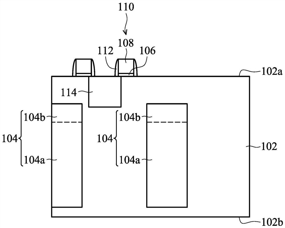
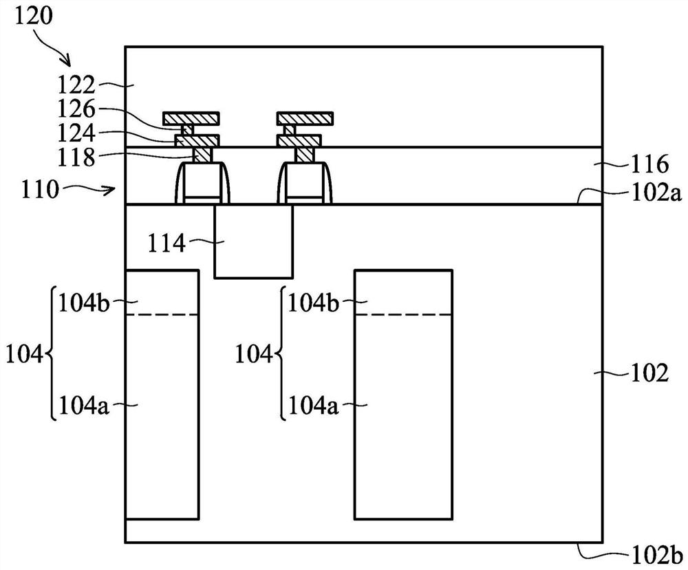
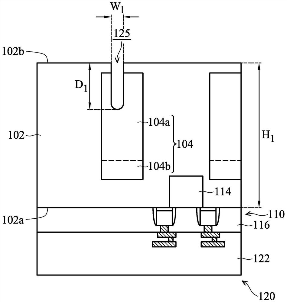
[0058] The following disclosure provides many different embodiments, or examples, of implementing different components of an embodiment of the invention. Examples of specific components and their arrangements are described below to simplify embodiments of the present invention. Of course, these are only examples and should not limit the scope of the embodiments of the present invention. For example, when the description mentions that a first element is formed on a second element, it may include embodiments where the first element is in direct contact with the second element, and may include other elements formed therebetween. And there is no example of direct contact. In addition, repeated symbols and / or symbols may be used in different embodiments, and these repetitions are only for simply and clearly describing the embodiments of the present invention, and do not represent a specific relationship between the different embodiments and / or structures discussed.

[0059] Some ...


PUM

PropertyMeasurementUnit
thicknessaaaaaaaaaa

Abstract

Embodiments of the present application provide an image sensor device structure and a forming method thereof. The image sensor device structure includes a substrate, and the substrate is doped with impurities of a first conductivity type. The image sensor device structure includes a photo-sensing region formed in the substrate, and the photo-sensing region is doped with impurities of a second conductivity type different from the first conductivity type. The image sensor device structure further includes a doping region extending into the photo-sensing region, and the doping region is doped with impurities of the first conductivity type. The image sensor device structure also includes a plurality of color filters formed on the doped regions.

Description

technical field [0001] Embodiments of the present invention relate to an image sensor device structure and a forming method thereof, and in particular to an image sensor device structure with a doped layer in a photo-sensing region. Background technique [0002] Semiconductor devices have been used in various electronic applications, such as personal computers, mobile phones, digital cameras, and other electronic equipment. The manufacture of semiconductor devices usually deposits various insulating or dielectric layers, conductive layers, and semiconductor layers of materials on a semiconductor substrate in sequence, and uses photolithography to pattern each material layer to form circuit elements and circuits thereon. components. Usually many integrated circuits are fabricated on a single semiconductor wafer, and individual dies on the wafer are diced between the integrated circuits along scribe lines. For example, individual dies are often individually packaged in multi...

Claims


Application Information

Patent Timeline
Patent Type & Authority Patents(China)
IPC IPC(8): H01L27/146
CPCH01L27/1461H01L27/14612H01L27/14621H01L27/14629H01L27/1463H01L27/14638H01L27/1464H01L31/03529H01L31/11H01L27/14643H01L27/14683H01L27/14685
Inventor 江彦廷陈春元曾晓晖王昱仁丁世汎吴尉壮刘人诚杨敦年
Owner TAIWAN SEMICON MFG CO LTD
Why Eureka
Try Eureka