Light sensing in display device

a display device and light sensing technology, applied in static indicating devices, instruments, electroluminescent light sources, etc., can solve the problems of display washed out, lack of color saturation, and loss of efficiency of oled display devices,

Inactive Publication Date: 2010-08-12
GLOBAL OLED TECH
View PDF8 Cites 104 Cited by
  • Summary
  • Abstract
  • Description
  • Claims
  • Application Information

AI Technical Summary

Benefits of technology

[0019]The present invention provides an integrated method employing an array of photosensors for ambient illumination...

Problems solved by technology

OLED display devices are subject to a loss of efficiency and light output as the organic materials age with time and use.
In general, the image quality of emissive display devices (such as OLED displays) suffers under bright ambient illumination.
In such conditions, the displays appear washed out and lacking in color saturation.
For active-matrix backplanes, providing photosensors within the pixel circuits limits the available technology employed to that of the thin-film material.
Amorphous silicon is known to unstable over time and low-temperature polysilicon is only available in small sizes and is known to have problems with non-uniformity.
The resulting circuits, b...

Method used


Image

  • Light sensing in display device
  • Light sensing in display device
  • Light sensing in display device

Examples


Embodiment Construction

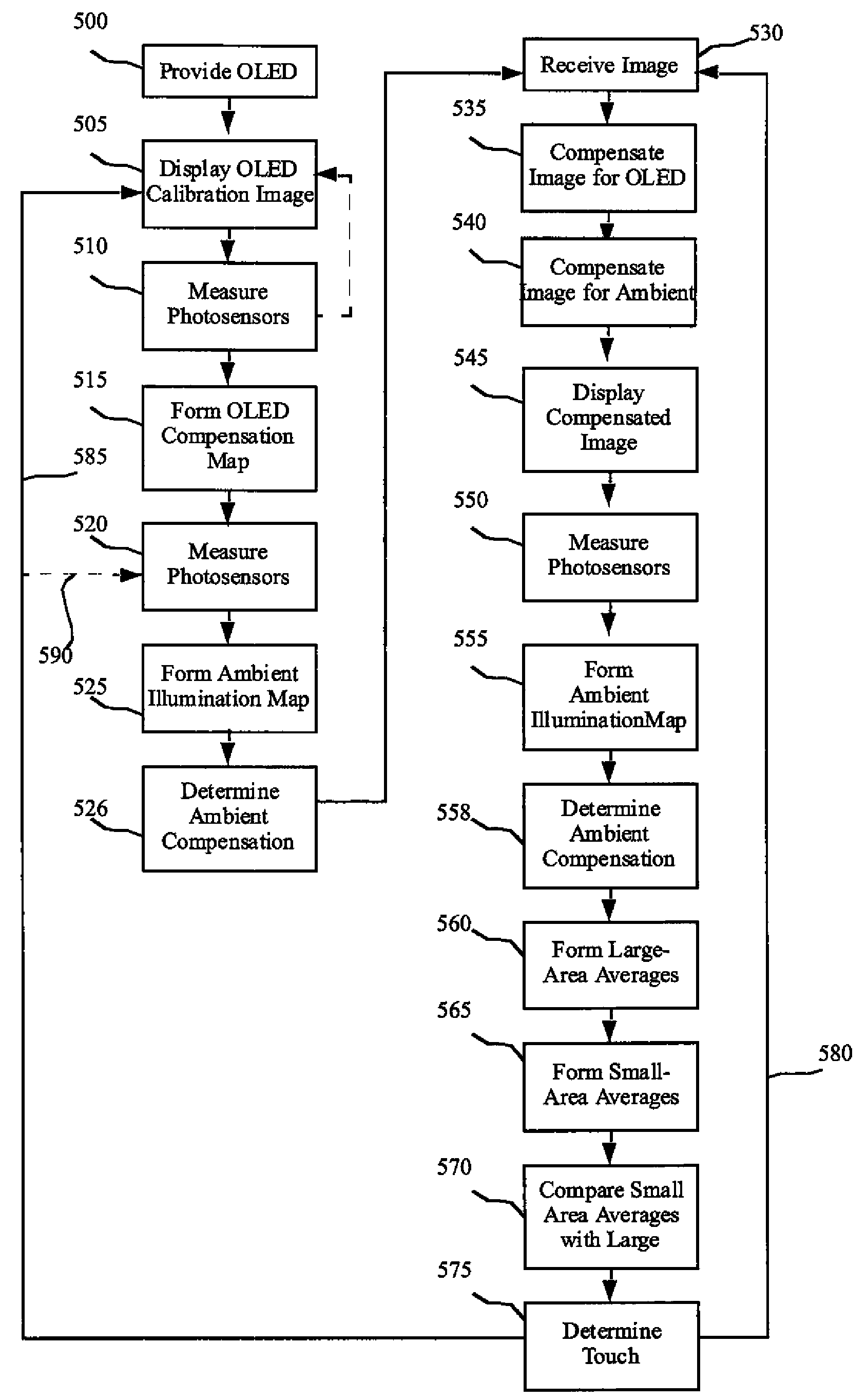
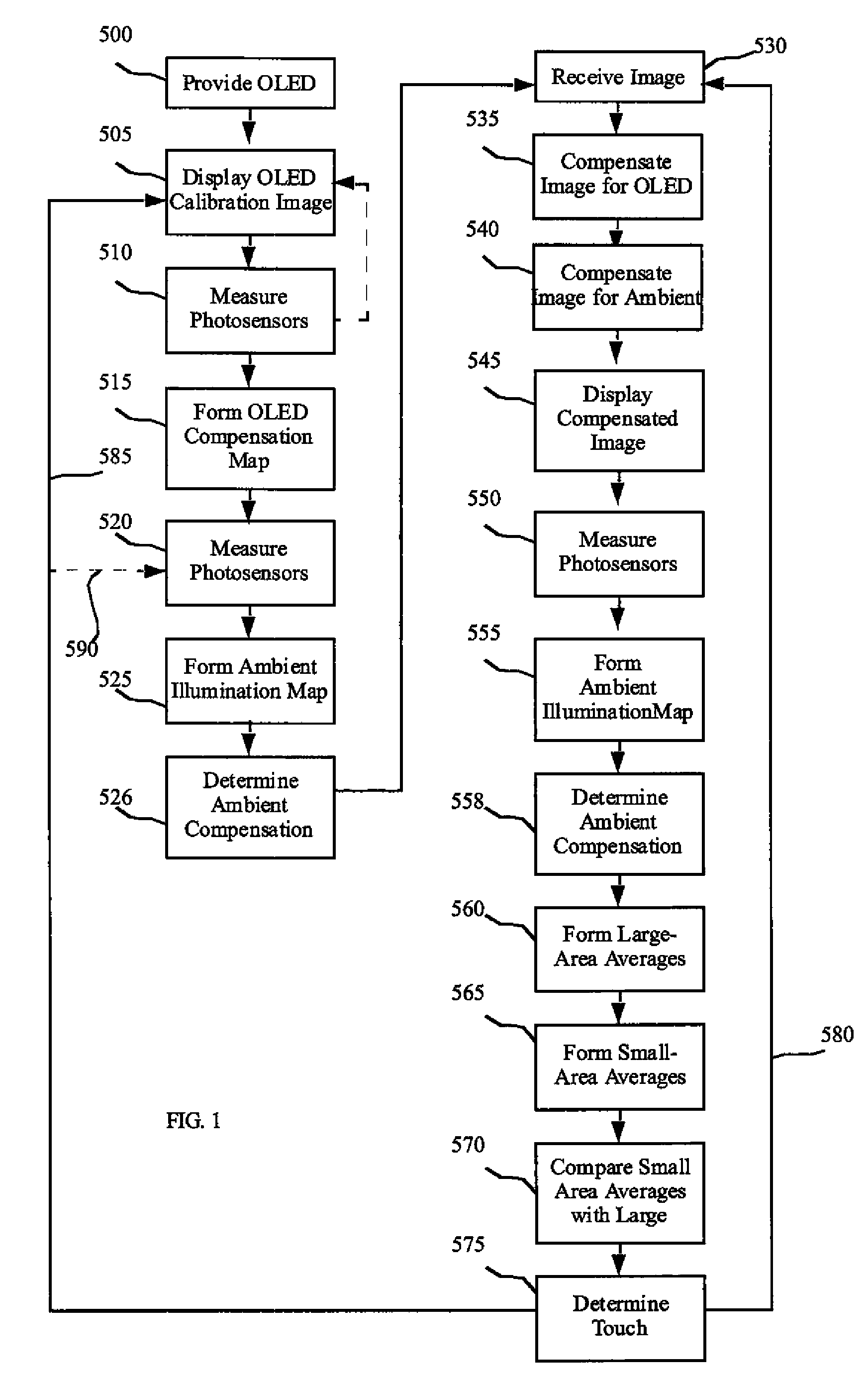
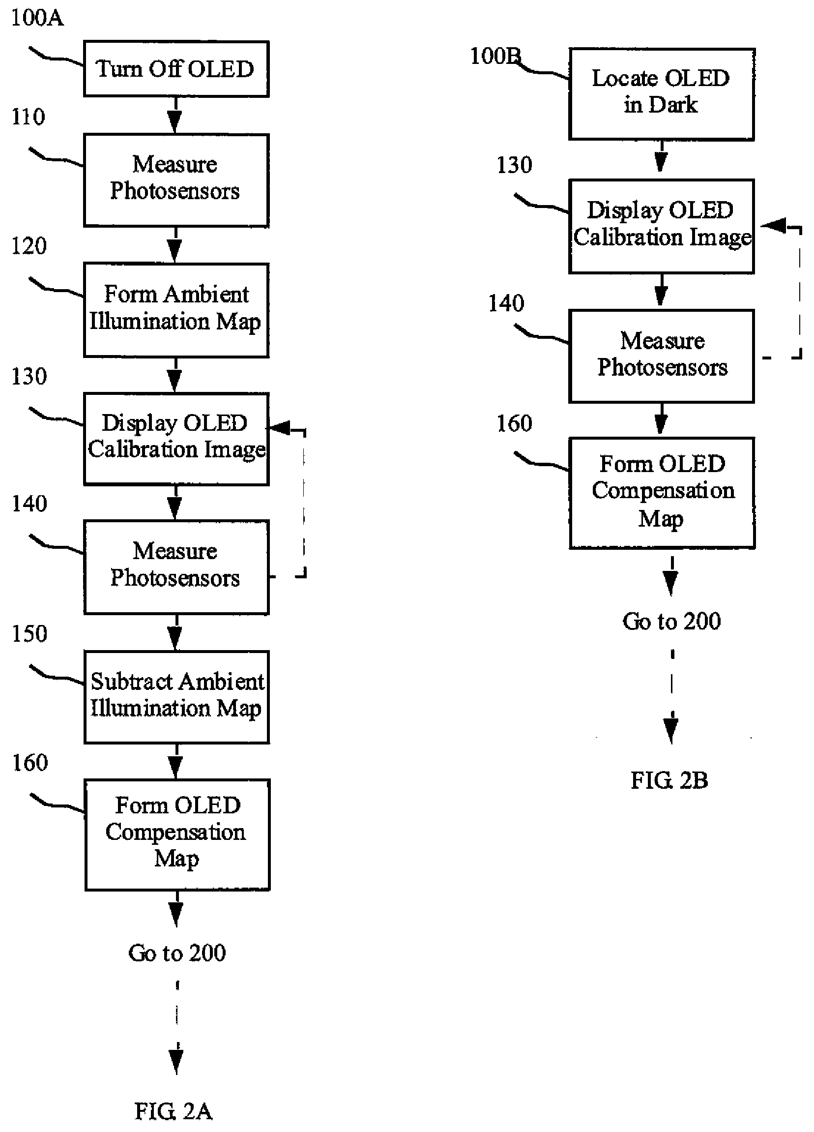
[0035]FIG. 1 includes a method for controlling an OLED display that is practiced by the external controller 60 shown in FIG. 6. In one embodiment of the present invention, the method includes providing 500 a substrate, an array of OLED pixels formed on the substrate forming a display area and having electrodes formed over the substrate. An array of photosensors distributed over the display area and supporting circuitry measures and communicates the ambient and emitted OLED light incident upon the photosensors. The OLED pixels are then driven 505 with at least one calibration image, a first incident light measurement made 510 and communicated to an external controller, and an OLED compensation map formed 515. These steps can be done initially in a manufacturing process, e.g. as part of a calibration process. This initial OLED compensation map can provide display non-uniformity correction and include any effects of factory burn-in, if performed on the OLED. The OLED calibration image ...


PUM


Abstract

A method for controlling an OLED display includes providing an OLED device and a controller, measuring and communicating the amount of ambient and emitted OLED light incident upon an array of photosensors distributed over the display area for measuring the incident light, operating the OLED pixels with at least one calibration image and forming an OLED compensation map in response to a first measured incident light, receiving a second incident light measurement and forming an ambient illumination map, receiving and compensating an image and driving the OLED pixels with the compensated image, receiving a third incident light measurement and forming large-area average values and small-area average values, and comparing the large-area average values and the small-area average values to a predetermined criterion, and determining the location of one or more light occlusions or reflections.

Description

FIELD OF THE INVENTION[0001]The present invention relates to a method for controlling an array of optical sensors in a display device having a substrate with distributed, independent chiplets for controlling a pixel array.BACKGROUND OF THE INVENTION[0002]Flat-panel display devices are widely used in conjunction with computing devices, in portable devices, and for entertainment devices such as televisions. Such displays typically employ a plurality of pixels distributed over a substrate to display images. Each pixel incorporates several, differently colored light-emitting elements commonly referred to as sub-pixels, typically emitting red, green, and blue light, to represent each image element. As used herein, pixels and sub-pixels are not distinguished and refer to a single light-emitting element. A variety of flat-panel display technologies are known, for example plasma displays, liquid crystal displays, and light-emitting diode (LED) displays.[0003]Light emitting diodes (LEDs) inc...

Claims


Application Information

Patent Timeline
IPC IPC(8): H05B37/02H05B44/00
CPCG06F3/0412H01L27/3269G06F3/042G09G3/2088G09G3/3225G09G2300/0426G09G2300/0819G09G2320/0209G09G2320/0233G09G2320/0295G09G2320/043G09G2320/0693G09G2360/144G09G2360/148G09G3/3208H01L27/3255G06F3/0418G06F3/04182H10K59/129H10K59/13G06F3/147
Inventor COK, RONALD S.HAMER, JOHN W.
Owner GLOBAL OLED TECH
Why Eureka
Try Eureka