Display apparatus having photo sensor

a technology of liquid crystal display and photo sensor, which is applied in the direction of identification means, instruments, radiation control devices, etc., can solve the problems of deteriorating visibility, limiting the display of high-quality images of transmissive and reflective liquid crystal display apparatuses

Active Publication Date: 2007-05-15
SAMSUNG DISPLAY CO LTD
View PDF3 Cites 102 Cited by
  • Summary
  • Abstract
  • Description
  • Claims
  • Application Information

AI Technical Summary

Benefits of technology

[0022]According to present invention, the light sensing part that senses an intensity of an ambient light is formed on the array substrate, so that a luminance of the display apparatus may be adjusted in accordance with the intensity of the ambient light.

Problems solved by technology

However, the organic electroluminescent display apparatus is one of the emissive display apparatuses, so that the organic electroluminescent display apparatus may not be formed in a reflective type.
Thus, when an environmental light is bright, a visibility is deteriorated.
Further, the transmissive and reflective type liquid crystal display apparatus has a limit to display a high quality image because the transmissive and reflective type liquid crystal display apparatus may not determine an intensity of the environmental light by itself.

Method used


Image

  • Display apparatus having photo sensor
  • Display apparatus having photo sensor
  • Display apparatus having photo sensor

Examples


embodiment 1

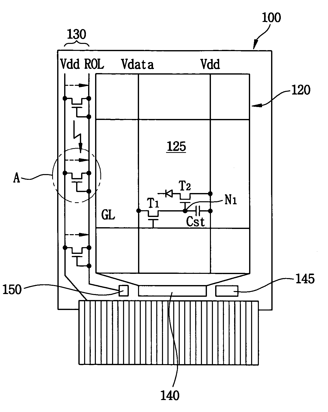
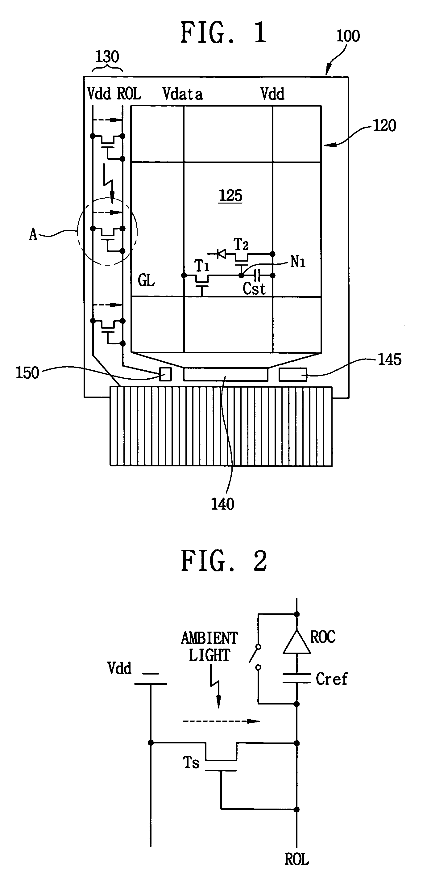
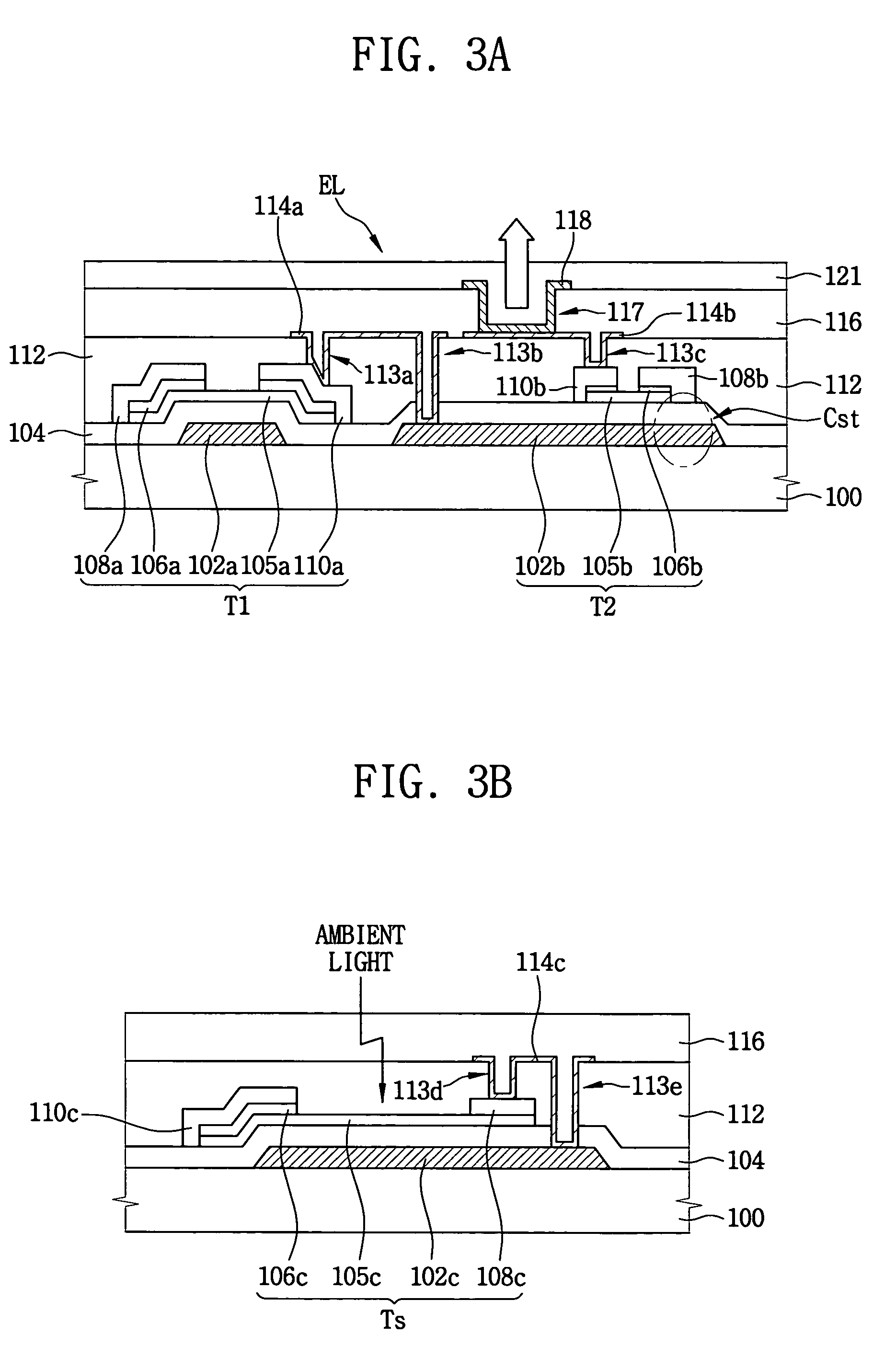
[0038]FIG. 1 is a schematic view showing a top emission type AMOELD apparatus according to a first exemplary embodiment of the present invention. FIG. 2 is an enlarged view showing a portion ‘A’ of FIG. 1. FIGS. 3A and 3B are cross-sectional views showing a pixel part and a light sensing part of the top emission type AMOELD of FIG. 1, respectively.

[0039]Referring to FIGS. 1, 2, 3A and 3B, a top emission type active matrix organic electroluminescence display apparatus (hereinafter, referred to as AMOELD) according to a first exemplary embodiment of the present invention includes an array substrate 100 having a plurality of pixels to display an image. The pixels are arranged in a matrix shape.

[0040]The array substrate includes a plurality of gate lines GL and a plurality of data lines Vdata. The gate lines GL and the data line Vdata are extended in a substantially perpendicular direction with each other to form a unit pixel 125 defined by the gate lines GL and the data lines Vdata.

[00...

embodiment 2

[0081]FIGS. 6A and 6B are cross-sectional views showing a pixel part and a light sensing part of an AMOELD according to a second exemplary embodiment of the present invention, respectively. The bottom type AMOELD of the present embodiment is same as in Embodiment 1 except for first and second electrodes. Thus, the same reference numerals will be used to refer to the same or like parts as those described in Embodiment 1 and any further explanation will be omitted.

[0082]Referring to FIGS. 6A and 6B, in case of a bottom emission type AMOELD, a light generated from an organic electroluminescent device EL exits the bottom type AMOELD via a substrate 100. Thus, the substrate 100 is disposed at a displaying side of the bottom type AMOELD.

[0083]Thus, the bottom type AMOELD includes a first electrode 114b that is transparent and operates as an anode electrode of an organic electroluminescent device EL, and a second electrode 121 that is opaque and operates as a cathode electrode of the organ...

embodiment 3

[0093]FIG. 7 is a schematic view showing a transmissive and reflective type liquid crystal display apparatus according to a third exemplary embodiment of the present invention, FIG. 8 is a circuit diagram showing a light sensing part of a transmissive and reflective type liquid crystal display apparatus according to a third exemplary embodiment of the present invention, and FIG. 9 is a cross-sectional view showing a light sensing part of the FIG. 8.

[0094]Referring to FIGS. 7, 8 and 9, a transmissive and reflective type liquid crystal display apparatus according to a third exemplary embodiment of the present invention includes an array substrate 200, a color filter substrate (not shown) facing the array substrate 200, and a liquid crystal layer (not shown) that is interposed between the array substrate 200 and the color filter substrate. A plurality of pixels is arranged in the array substrate 200.

[0095]A gate line GL and a data line Vdata formed in a display region of the array subs...


PUM

PropertyMeasurementUnit
voltageaaaaaaaaaa
voltageaaaaaaaaaa
photocurrentaaaaaaaaaa

Abstract

An electronic display apparatus includes a substrate, pixels and light sensing parts. The substrate includes a display region and a peripheral region adjacent the display region, and the substrate includes a plurality of gate lines extended in a first direction and a plurality of data lines extended in a second direction that is substantially perpendicular to the first direction. The pixels defined by each of the data and gate lines are formed in the display region to display an image. The light sensing part is formed in the peripheral region, and the light sensing part senses an intensity of an ambient light. The light sensing part that senses an intensity of an ambient light is formed on the array substrate, so that a luminance of the display apparatus may be adjusted in accordance with the intensity of the ambient light.

Description

CROSS-REFERENCE TO RELATED APPLICATIONS[0001]This application relies for priority upon Korean Patent Application No. 2003-71871 filed on Oct. 15, 2003, the contents of which are herein incorporated by reference in its entirety.BACKGROUND OF THE INVENTION[0002]1. Field of the Invention[0003]The present invention relates to a display apparatus, and more particularly to a display apparatus having photo sensor formed on a substrate on which pixel arrays are formed.[0004]2. Description of the Related Art[0005]In the information society at the present time, electronic display apparatuses are more important as information transmission media and various electronic display apparatuses are widely applied for industrial apparatus or home appliances. Such electronic display apparatuses continue to advance to have new appropriate functions for various demands of the information society.[0006]In general, electronic display apparatuses display and transmit various pieces of information to users wh...

Claims


Application Information

Patent Timeline
Patent Type & Authority Patents(United States)
IPC IPC(8): H05B33/00G02F1/1345G02F1/133G09F9/00G09F9/30G09F9/33G09F9/35G09G3/20G09G3/32H01J1/62H01J63/04H01L27/144H01L27/146H01L27/30H01L27/32H01L31/105H01L51/50H01L51/52H05B33/14
CPCG09G3/3225H01L27/1446H01L27/3269H01L31/1055G02F2201/58G09G2300/0842G09G2320/0626G09G2360/144G09G2360/148H01L27/14692H01L27/30H01L51/5284H01L2251/5315H10K39/00H10K59/13H10K50/865H10K2102/3026G09G3/20
Inventor CHOI, JOON-HOOJOO, IN-SUCHUNG, KYU-HA
Owner SAMSUNG DISPLAY CO LTD
Why Eureka
Try Eureka