A kind of pixel structure and transfer method of micro-light-emitting diode

A technology of micro light-emitting diode and pixel structure, applied in the field of pixel structure, can solve the problems of the influence of the deformation of the transfer backplane, the deterioration of display uniformity, the large size of the transfer backplane, etc., and achieve the effect of realizing production economy.

Inactive Publication Date: 2019-08-02
NANJING CEC PANDA LCD TECH
View PDF10 Cites 0 Cited by
  • Summary
  • Abstract
  • Description
  • Claims
  • Application Information

AI Technical Summary

Problems solved by technology

[0003] For large-size micro-LED display panels, there are currently three technical solutions to this problem: the first solution is to increase the size of the transfer backplane as much as possible, and realize the large-size micro-light-emitting diode display panel through one transfer as much as possible. In theory, this solution can reduce the number of transfers and improve the transfer accuracy, but the larger the size of the transfer backplane, the higher the requirements for the stability and control accuracy of the transfer equipment, and if the size of the transfer backplane is too large, it will It leads to bending and deformation, which eventually leads to the deviation of the position of the micro-light emitting diode, and the uniformity of the display is deteriorated, and the large-size transfer backplane is greatly affected by external environmental factors, and the temperature and humidity will have deformation effects on the large-size transfer backplane. Thus ultimately affecting the display effect of the display panel
[0004] The second approach is to use a patterned sacrificial layer to form a direct alignment metallization stack and use the patterned sacrificial layer as an etch stop layer during etching of the p-n diode layer to form multiple micro p-n diodes. method, the etching process will produce a certain tolerance, and the etching also has higher requirements for the combination of the micro-light emitting diode and the display panel. If the combination is not tight, it will fall off during the etching process. At the same time, using this solution, the micro-LEDs fall off, and this solution cannot be repaired again
[0005] The third solution is to transfer multiple times directly on the large-size micro-LED backplane, and finally manufacture a large-size micro-LED panel. This solution is currently the most economical solution, but due to multiple transfers, This puts forward very high requirements on the alignment accuracy of the micro-LEDs transferred each time. In the prior art, the method of setting grooves and protrusions is generally used for transfer, but in this process, the positioning accuracy cannot be guaranteed. , and making grooves and bumps will increase the manufacturing cost

Method used


Image

  • A kind of pixel structure and transfer method of micro-light-emitting diode
  • A kind of pixel structure and transfer method of micro-light-emitting diode
  • A kind of pixel structure and transfer method of micro-light-emitting diode

Examples


Embodiment

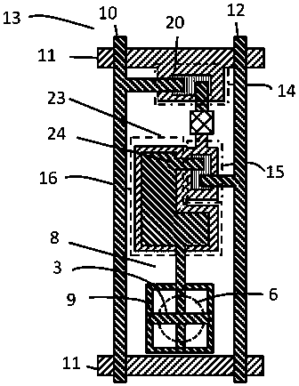
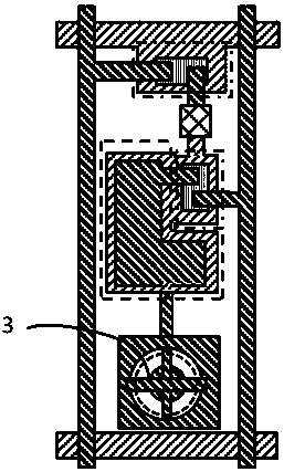
[0050] Figure 2-7 It is a schematic diagram of the pixel structure of the micro light-emitting diode of the present invention, Figure 8-9 It is a schematic side view of the bonding metal part of the micro light emitting diode of the present invention, Figure 10 It is a circuit diagram of the micro light emitting diode of the present invention.

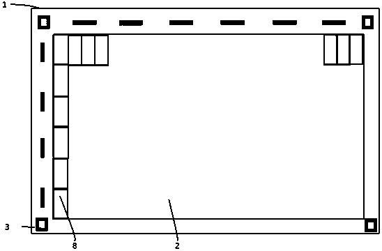
[0051] like figure 2 As shown, a pixel structure includes data lines 10 and power lines 12 vertically arranged on the substrate 13, scanning lines 11 arranged laterally on the substrate 13 and perpendicular to the data lines 10 and scanning lines 12, composed of scanning lines 11, The pixel area 8 formed by the data line 10 and the power line 12 criss-crossing, the capacitor electrode 16 located in the pixel area 8, the first thin film transistor switch 14 and the second thin film transistor switch located in the pixel area 8 and connected to the capacitor electrode 16 15. The bonding metal layer 9 located in the pixel area 8 an...


PUM


Abstract

The invention discloses a pixel structure and a transfer method of a micro light-emitting diode, belonging to the field of display panel manufacturing. The invention discloses a pixel structure, which includes: criss-cross data lines and scan lines, and power lines parallel to the data lines , a pixel area formed by scanning lines, data lines and power lines, and a capacitor electrode located in the pixel area, and a bonding metal layer located in the pixel area and connected to the capacitor electrode, and a bonding metal layer arranged in the bonding metal layer Alignment mark, in the present invention, the alignment mark is set on the bonding metal layer, and the alignment operation is performed through the micro-light emitting diode and the alignment mark, which can ensure the alignment accuracy during the transfer process of the micro-light-emitting diode, and at the same time does not affect the micro-light emitting diode. The driving of the light-emitting diode does not add any other structure, does not change the existing manufacturing process, does not add a new process, and realizes economical production.

Description

technical field [0001] The invention relates to a pixel structure, in particular to a pixel structure and a transfer method of a micro light emitting diode. Background technique [0002] At present, the transfer technology of Micro LED varies according to the size of the panel, such as figure 1 Shown is a schematic diagram of a micro-LED panel in the prior art. For a small-sized micro-LED panel 1, the transfer substrate (not shown) can transfer all micro-LEDs (not shown) in all pixel regions 8 at one time. Therefore, for a small-sized micro-LED panel 1, it is only necessary to set alignment marks 3 around the periphery of the display area 2 to achieve precise alignment of the micro-LEDs. This solution is suitable for small-sized wearable devices and does not It is suitable for large-sized micro light-emitting diode display panels. [0003] For large-size micro-LED display panels, there are currently three technical solutions to this problem: the first solution is to increa...

Claims


Application Information

Patent Timeline
Patent Type & Authority Patents(China)
IPC IPC(8): G09F9/33H01L21/68H01L21/677H01L27/15H01L21/683
Inventor 朱景辉王鸣昕黄洪涛徐尚君高威
Owner NANJING CEC PANDA LCD TECH
Why Eureka
Try Eureka