Printed circuit board manufacturing method and printed circuit board

A printed circuit board and manufacturing method technology, applied in the directions of printed circuit components, multilayer circuit manufacturing, etc., can solve the problems of human target selection errors, alignment errors, product scrap, etc., to achieve high reliability and reduce alignment errors. , the effect of improving production efficiency

Active Publication Date: 2014-10-22
NEW FOUNDER HLDG DEV LLC +1
View PDF5 Cites 11 Cited by
  • Summary
  • Abstract
  • Description
  • Claims
  • Application Information

AI Technical Summary

Problems solved by technology

In the base-level alignment method, since all the alignment targets of the build-up layer are formed on the substrate and have the same reference system, the alignment accuracy is relatively high; Because of the target as the alignment benchmark for all build-up layers, it is easy to make human-made target selection errors, resulting in alignment errors, resulting in product scrapping

Method used


Image

  • Printed circuit board manufacturing method and printed circuit board
  • Printed circuit board manufacturing method and printed circuit board
  • Printed circuit board manufacturing method and printed circuit board

Examples


Embodiment 1

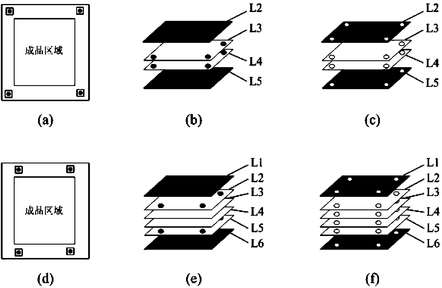
[0062] Such as image 3 As shown, in this embodiment, the substrate adopts a double-sided substrate, and the printed circuit board produced is a six-layer HDI printed circuit board, and two layers of build-up layers are respectively arranged on both sides of the double-sided substrate (that is, a total of four layers of build-up layers) . The manufacturing method of this six-layer HDI printed circuit board comprises the steps:

[0063] A1. A group of first targets are respectively set at the three corners of the double-sided substrates L3 and L4, and a pair of first targets is set at the corners of the substrates where the first target is not set. A secondary target for bit benchmarks.

[0064] In this step, the first target, the second target used as an alignment reference for the build-up layer adjacent to the double-sided substrate, and the pattern on the substrate are simultaneously formed on the double-sided substrate by pattern transfer superior. At this time, the f...

Embodiment 2

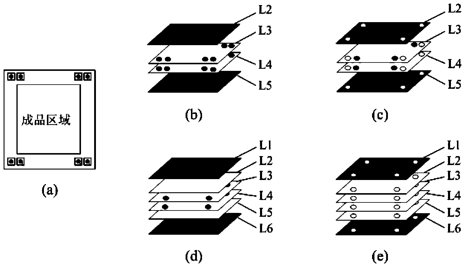
[0085] The printed circuit board in this embodiment is a seven-layer HDI printed circuit board. If a double-sided substrate is also used, the number of build-up layers to be set is five, and the five-layer build-up layers are asymmetrically distributed on both sides of the double-sided substrate. , for example, a double-sided substrate with a three-layer buildup on one side and a two-layer buildup on the other side. The manufacturing method of this seven-layer HDI printed circuit board comprises the following steps:

[0086] A1. A set of first targets are respectively arranged on the double-sided substrates, and a second target used as an alignment reference for a build-up layer adjacent to the double-sided substrates is arranged at a corner of the substrate where no first targets are arranged.

[0087] In this step, when the number of build-up layers to be set is asymmetrically distributed on both sides of the substrate, the number of first targets in the group of first targ...

Embodiment 3

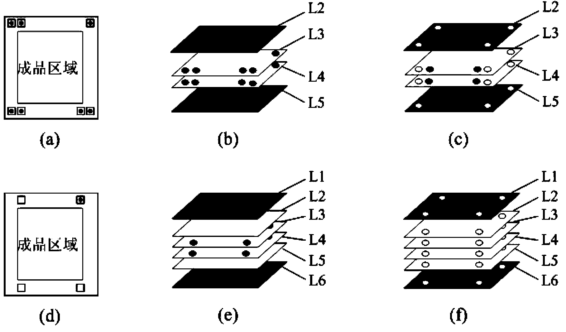
[0099] The difference between this embodiment and Embodiments 1 and 2 is that the printed circuit board of this embodiment is laminated with build-up only on one side of the double-sided substrate, or the substrate itself is a single-sided substrate, and the build-up is laminated only on one side. .

[0100] In this embodiment, after each build-up layer is pressed on the side of the substrate where the build-up layer needs to be pressed, the second target on the substrate or the build-up layer and the unused target corresponding to the second target on the substrate and the same build-up layer The used first target is used as a reference to form a target hole on one of the laminated build-up layers; and using the target hole as an alignment reference, pattern transfer is performed on one of the laminated build-up layers until completion Pattern transfer of all buildup layers on one side of the substrate.

[0101] In this embodiment, the specific steps of the printed circuit b...


PUM


Abstract

The invention relates to a printed circuit board manufacturing method and a printed circuit board. The printed circuit board manufacturing method comprises the following steps: a group of first targets is arranged in at least one corner of a substrate, and a second target used as an alignment benchmark for a build-up layer adjacent to the substrate is arranged in a corner of the substrate not equipped with a first target; the build-up layer is press-fitted, and a target hole is formed in a corresponding position of the build-up layer with the second target and the first target which is arranged on the substrate and corresponds to the same build-up layer as the second target as a benchmark; and with the target hole as an alignment benchmark, graphic transfer is performed on the build-up layer where the target hole is arranged, and graphic transfer further includes the step of forming a second target used as an alignment benchmark for a relatively outer build-up layer on the build-up layer where the target hole is arranged; and the previous two steps are repeated to complete manufacture of a printed circuit board. The method effectively reduces possible alignment error in the process of high-order HDI printed circuit board manufacturing, and improves the reliability of the product.

Description

technical field [0001] The invention belongs to the technical field of printed circuit board manufacturing, and in particular relates to a method for manufacturing a printed circuit board and a printed circuit board manufactured by the method. Background technique [0002] Printed circuit board (PCB, Printed Circuit Board), also known as printed circuit board, is a provider of electrical connections for electronic components. It uses an insulating board as the base material, and at least one conductive pattern is attached to it, and holes (such as component holes, fastening holes, metallized holes, etc.) are used to replace the chassis of the previous electronic components and realize electronic components. Interconnection between components. [0003] With the continuous development of the printed circuit board industry, the number of layers of printed circuit boards is increasing, and the circuits are becoming more and more complex. High-density interconnection technology ...

Claims


Application Information

Patent Timeline
Patent Type & Authority Applications(China)
IPC IPC(8): H05K3/46H05K1/02
Inventor 陈臣郑志军
Owner NEW FOUNDER HLDG DEV LLC
Why Eureka
Try Eureka