Display control method
A display, control field technology, applied in the direction of static indicators, instruments, etc.
- Summary
- Abstract
- Description
- Claims
- Application Information
AI Technical Summary
Problems solved by technology
Method used
Image
Examples
Embodiment Construction
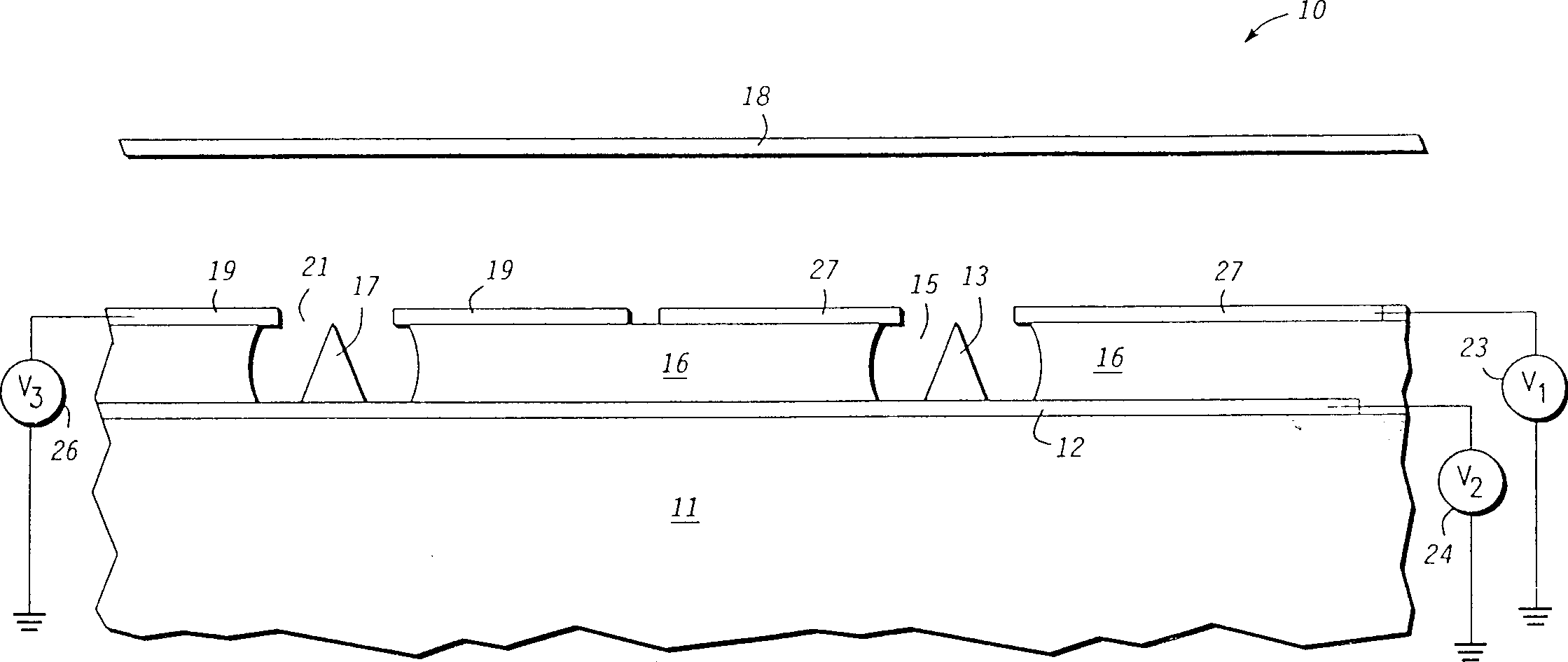
[0008] figure 1 An enlarged cross-sectional view of a field emission device display 10 utilizing matrix addressing is schematically shown. The display 10 includes a substrate 11 on which other parts of the display 10 are formed. Generally, the substrate 11 is an insulating or semi-insulating material, such as a silicon material with a dielectric layer or glass. In a preferred embodiment, substrate 11 is glass. Typically, a cathode conductor or column 12 is formed on the surface of substrate 11 by which emitter tips or electrodes 13 and 17 are connected to a column of display 10 . The material used for column 12 may be a metal or a low resistance layer such as doped polysilicon. The first extraction gate or row 27 and the second extraction gate or row 19 are electrically isolated from the substrate 11 and the columns 12 by means of the dielectric layer 16 . Electrons are emitted by the emitters 13 and 17, and the emitted electrons are collected by the anode 18 disposed at a...
PUM
 Abstract
Description
Claims
Application Information


