PCB detection method and device and computer readable storage medium

A technology of PCB board and detection method, which is applied in the directions of calculation, optical test defect/defect, image analysis, etc., can solve the problem of low efficiency of PCB back drilling, improve test efficiency and accuracy, improve accuracy, avoid inefficient effect

Pending Publication Date: 2019-06-21
SHENZHEN EAGLE EYE ONLINE ELECTRONICS TECH
View PDF4 Cites 12 Cited by
  • Summary
  • Abstract
  • Description
  • Claims
  • Application Information

AI Technical Summary

Problems solved by technology

[0005] The main purpose of the present invention is to provide a PCB board detection method, device and computer-readable storage medium,

Method used


Image

  • PCB detection method and device and computer readable storage medium
  • PCB detection method and device and computer readable storage medium
  • PCB detection method and device and computer readable storage medium

Examples


no. 1 example

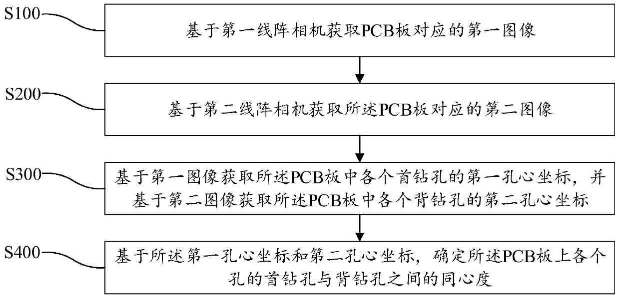
[0098]Based on the first embodiment, the second embodiment of the PCB board detection method of the present invention is proposed. In this embodiment, the PCB board is provided with positioning holes; step S300 includes:

[0099] Step S310, aligning the first image and the second image based on the positioning hole;

[0100] Step S320: Obtain the first hole center coordinates of each first drilled hole in the PCB board based on the first image after alignment, and obtain the second coordinates of each back-drilled hole in the PCB board based on the second image after alignment. Hole center coordinates.

[0101] In this embodiment, after the first image and the second image are obtained, the positioning hole corresponding to the PCB board is obtained, and the first image and the second image are aligned according to the positioning hole, and then according to the aligned first image The first hole center coordinates corresponding to the PCB board are obtained from an image, an...

no. 3 example

[0112] Based on the third embodiment, the fourth embodiment of the PCB detection method of the present invention is proposed. In this embodiment, step S430 includes:

[0113] Step S431, determining whether there is a target distance greater than a preset distance in the minimum distance;

[0114] Step S432, if it does not exist, then determine the coordinates of the first drilled hole and the coordinates of the back drilled hole corresponding to each hole on the PCB based on the distance;

[0115] Step S433, if it exists, then output the first prompt information that the PCB board is unqualified.

[0116] In this embodiment, when determining the minimum distance, it is determined whether there is a target distance greater than the preset distance in the minimum distance, and it has been determined whether the PCB board is an unqualified PCB board according to the preset distance, and there is a target distance greater than the preset distance in the minimum distance. When the...


PUM


Abstract

The invention discloses a PCB detection method. The method comprises the steps of obtaining a first image corresponding to a PCB based on a first linear array camera; Acquiring a second image corresponding to the PCB based on a second linear array camera; Obtaining a first hole center coordinate of each first drill hole in the PCB based on the first image, and obtaining a second hole center coordinate of each back drill hole in the PCB based on a second image; And based on the first hole center coordinate and the second hole center coordinate, determining the concentricity between the first drill hole and the back drill hole of each hole in the PCB. The invention also discloses a PCB detection device and a computer readable storage medium. The concentricity of the PCB back drilled hole andthe first drilled hole is detected through image recognition, the concentricity of all the back drilled holes and the first drilled hole in the PCB can be detected at the same time through the firstimage and the second image, and the problem that manual quadratic element detection is low in efficiency is solved.

Description

technical field [0001] The invention relates to the technical field of PCB boards, in particular to a PCB board detection method, device and computer-readable storage medium. Background technique [0002] In the prior art, in the production process of PCB board (Printed Circuit Board, printed circuit board), when carrying out PCB board detection, need to detect the concentricity between the back drilling hole of PCB board and the first drilling hole, in order to Prevent the outflow of products that do not meet the processing requirements. [0003] At present, manual methods are generally used, and at the same time, artificial secondary element detection is carried out with the help of instruments such as scales. It is difficult and inefficient to detect concentricity manually. In addition, manual two-dimensional inspection can only detect the concentricity of one back-drilled hole at a time. When the number of back-drilled holes on the PCB is large, the manual workload and...

Claims


Application Information

Patent Timeline
IPC IPC(8): G06T7/00G06T7/60G06T7/70G01N21/88
Inventor 周翔郑如寿李小明
Owner SHENZHEN EAGLE EYE ONLINE ELECTRONICS TECH
Why Eureka
Try Eureka