Touch display device
A touch display device and conductive electrode technology, which can be used in instruments, computing, electrical digital data processing, etc., can solve problems such as interference fringes and penetration rate effects, and achieve the effect of preventing interference fringes.
- Summary
- Abstract
- Description
- Claims
- Application Information
AI Technical Summary
Problems solved by technology
Method used
Image

Examples
no. 1 example
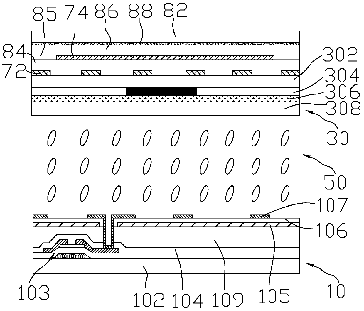
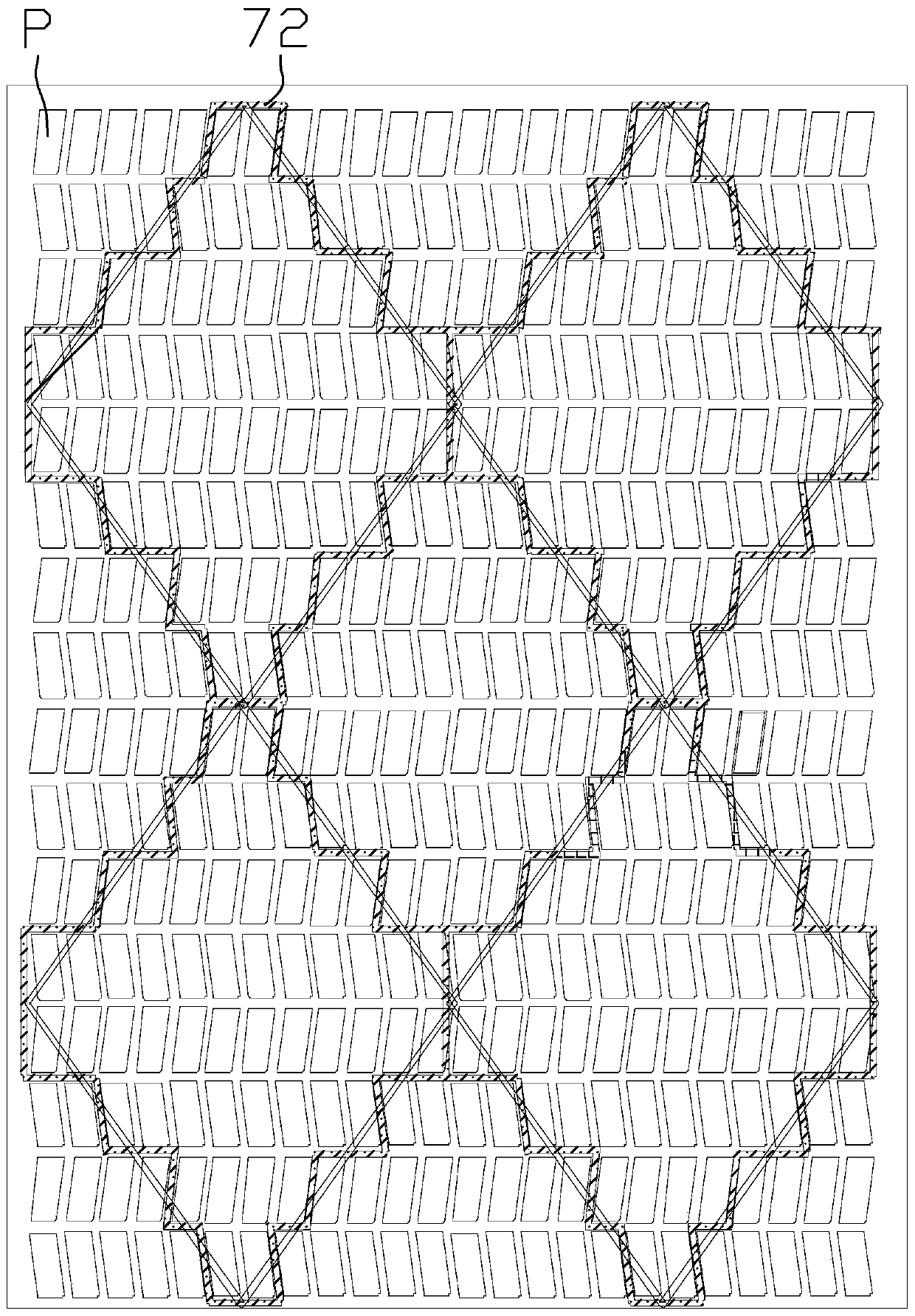
[0032] Such as figure 1 As shown, the touch display device according to the first embodiment of the present invention includes a first substrate 10 , a second substrate 30 opposite to the first substrate 10 , and a liquid crystal between the first substrate 10 and the second substrate 30 Layer 50. The first substrate 10 includes a first substrate 102, a switching element 103, a first insulating layer 104, a first electrode layer 105, a second insulating layer 106, and a second electrode layer 107, the switching element 103, the first insulating layer 104, the second An electrode layer 105 , a second insulating layer 106 and a second electrode layer 107 are sequentially stacked on the surface of the first substrate 102 facing the liquid crystal layer 50 . A plurality of pixel units P are also formed on the first substrate defined by scan lines and data lines (see figure 2 ). The second substrate 30 includes a second base 302 , a light-shielding structure 304 and a color-res...
no. 2 example
[0044] Such as Figure 4 As shown, the touch display device according to the second embodiment of the present invention includes a first substrate 10 , a second substrate 30 opposite to the first substrate 10 , and a liquid crystal between the first substrate 10 and the second substrate 30 Layer 50. The first substrate 10 includes a first substrate 102, a switching element 103, a first insulating layer 104, a first electrode layer 105, a second insulating layer 106, a second electrode layer 107, and a third insulating layer 108. The switching element 103, the first insulating layer An insulating layer 104 , a first electrode layer 105 , a second insulating layer 106 , a second electrode layer 107 and a third insulating layer 108 are sequentially stacked on the surface of the first substrate 102 facing the liquid crystal layer 50 . A plurality of pixel units P are formed on the first substrate defined by scan lines and data lines. The second substrate 30 includes a second bas...
no. 3 example
[0048] Such as Figure 5 As shown, the structure of the touch display device of the third embodiment of the present invention is basically the same as that of the touch display device of the second embodiment. The difference is that in the third embodiment, the second conductive electrode 74 is arranged on the second substrate 302 is away from the side of the liquid crystal layer 50 . Other structures of the touch display device of this embodiment are the same as those of the touch display device of the second embodiment, and will not be repeated here.
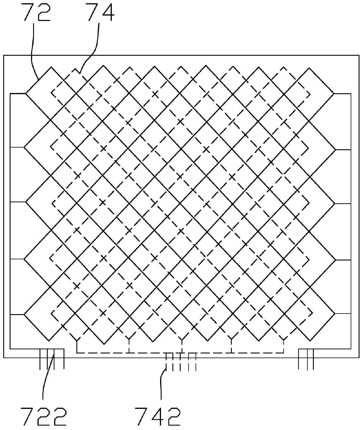
[0049] In the touch display device of the present invention, the Metal Mesh process is used to form the first conductive electrode 72 as the touch driving electrode and the second conductive electrode 74 as the touch sensing electrode, and the first conductive electrode 72 and the second conductive electrode 74 are formed in a diamond grid. Both of the two conductive electrodes 74 correspond to the area of the light-shieldi...
PUM
 Abstract
Description
Claims
Application Information
 - R&D
- Intellectual Property
- Life Sciences
- Materials
- Tech Scout
- Unparalleled Data Quality
- Higher Quality Content
- 60% Fewer Hallucinations
Browse by: Latest US Patents, China's latest patents, Technical Efficacy Thesaurus, Application Domain, Technology Topic, Popular Technical Reports.
© 2025 PatSnap. All rights reserved.Legal|Privacy policy|Modern Slavery Act Transparency Statement|Sitemap|About US| Contact US: help@patsnap.com