Supercharge Your Innovation With Domain-Expert AI Agents!

Structure of static random access memory and formation method thereof

A static random access and memory technology, which is applied in semiconductor/solid-state device manufacturing, semiconductor devices, electric solid-state devices, etc., can solve the conflict between static random access memory writeability and read stability, static random access memory poor performance

Active Publication Date: 2019-07-05
SEMICONDUCTOR MANUFACTURING INTERNATIONAL (BEIJING) CORP +1
View PDF8 Cites 0 Cited by
  • Summary
  • Abstract
  • Description
  • Claims
  • Application Information

AI Technical Summary

Problems solved by technology

Therefore, the different requirements for the performance of the pass transistor cause a conflict between the writeability and read stability of the SRAM
[0004]However, prior art SRAM performance is still poor

Method used


Image

  • Structure of static random access memory and formation method thereof
  • Structure of static random access memory and formation method thereof
  • Structure of static random access memory and formation method thereof

Examples


Embodiment Construction

[0027] As mentioned in the background, the performance of the static random access memory formed by the prior art is relatively poor.

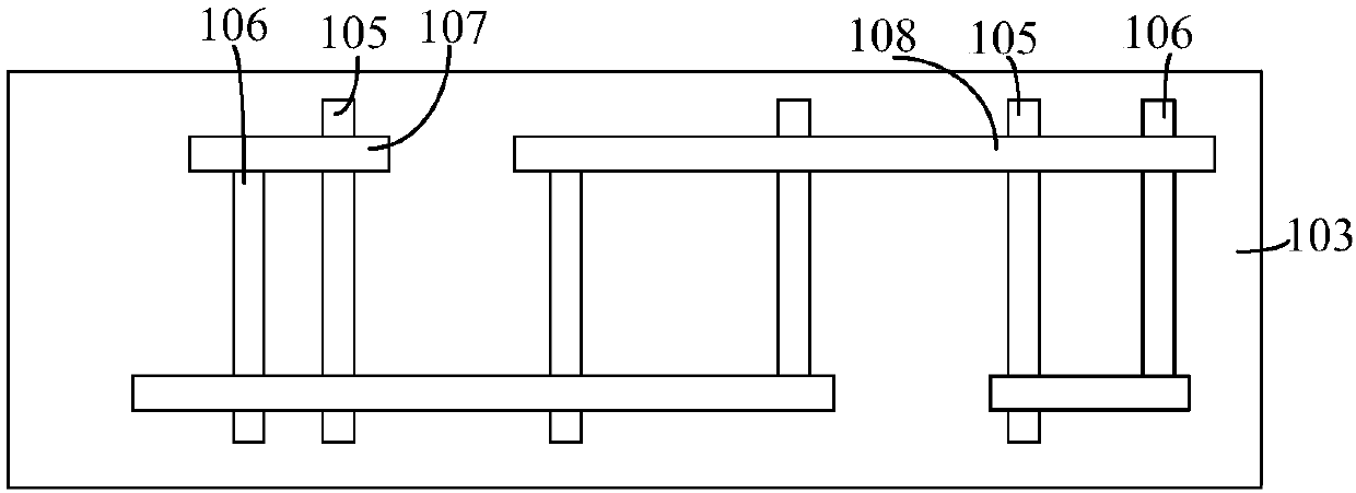
[0028] figure 1 It is a schematic diagram of the structure of a static random access memory.

[0029] Please refer to figure 1 , the base 100; the first fin 105 and the second fin 106 located on the surface of the base 100; the first gate structure 107 across the first fin 105; the first fin 105 across the second fin 106 The second gate structure 108; the first source-drain doped region (not shown in the figure) located in the first fin portion 105 on both sides of the first gate structure 107; located on both sides of the second gate structure 108 The second source-drain doped region (not shown in the figure) in the first fin portion 105 and the second fin portion 106 .

[0030] In the above method, the same patterning process is used to form the first fin portion 105 and the second fin portion 106 , so that the width difference between th...


PUM


Abstract

The present invention provides a structure of a static random access memory and a formation method thereof. The method comprises the steps of: providing an initial substrate, wherein the initial substrate comprises at least one first region; removing part of the initial substrate of the at least one first region, and forming a substrate, a first fin portion located at the surface of the substrateand a second initial fin portion located at the surface of the substrate, wherein the second initial fin portion and the first fin portion are different in width, part of the first fin portion is configured to form pass-gate transistors, and part of the first fin portion and the second initial fin portion are configured to form pull-down transistors. The static random access memory formed by employing the method is good in performance.

Description

technical field [0001] The invention relates to the technical field of integrated circuits, in particular to a structure of a static random access memory and a forming method thereof. Background technique [0002] With the continuous development of digital integrated circuits, on-chip integrated memory has become an important part of digital systems. Static Random Access Memory (SRAM) has become an indispensable and important part of on-chip memory due to its advantages of low power consumption and high speed. SRAM can hold data as long as power is supplied to it, rather than constantly refreshing it. [0003] The basic SRAM generally includes six transistors: 2 pull-up transistors (Pull-up transistor, PU), 2 pull-down transistors (Pull-down transistor, PD) and 2 pass-gate transistors (Pass-gate transistor, PG) . In the neural process of SRAM, it is usually necessary to ensure a sufficiently large β ratio (Ipd / Ipg current ratio) to obtain a sufficiently high static noise ...

Claims


Application Information

Patent Timeline
IPC IPC(8): H01L21/8244H01L27/11
CPCH10B10/12H01L21/31111H01L21/31155H01L21/3086H01L21/26506
Inventor 王楠
Owner SEMICONDUCTOR MANUFACTURING INTERNATIONAL (BEIJING) CORP
Features
  • R&D
  • Intellectual Property
  • Life Sciences
  • Materials
  • Tech Scout
  • Unparalleled Data Quality
  • Higher Quality Content
  • 60% Fewer Hallucinations
Learn More