Image sensors with calibrated phase detection pixels, and operation method thereof

An image sensor and phase detection technology, applied in the field of imaging systems, which can solve problems such as inaccurate and inconsistent depth calculations

Inactive Publication Date: 2019-07-05
SEMICON COMPONENTS IND LLC
View PDF9 Cites 1 Cited by
  • Summary
  • Abstract
  • Description
  • Claims
  • Application Information

AI Technical Summary

Problems solved by technology

This can lead to inaccurate and inconsistent depth calculations

Method used


Image

  • Image sensors with calibrated phase detection pixels, and operation method thereof
  • Image sensors with calibrated phase detection pixels, and operation method thereof
  • Image sensors with calibrated phase detection pixels, and operation method thereof

Examples


Embodiment Construction

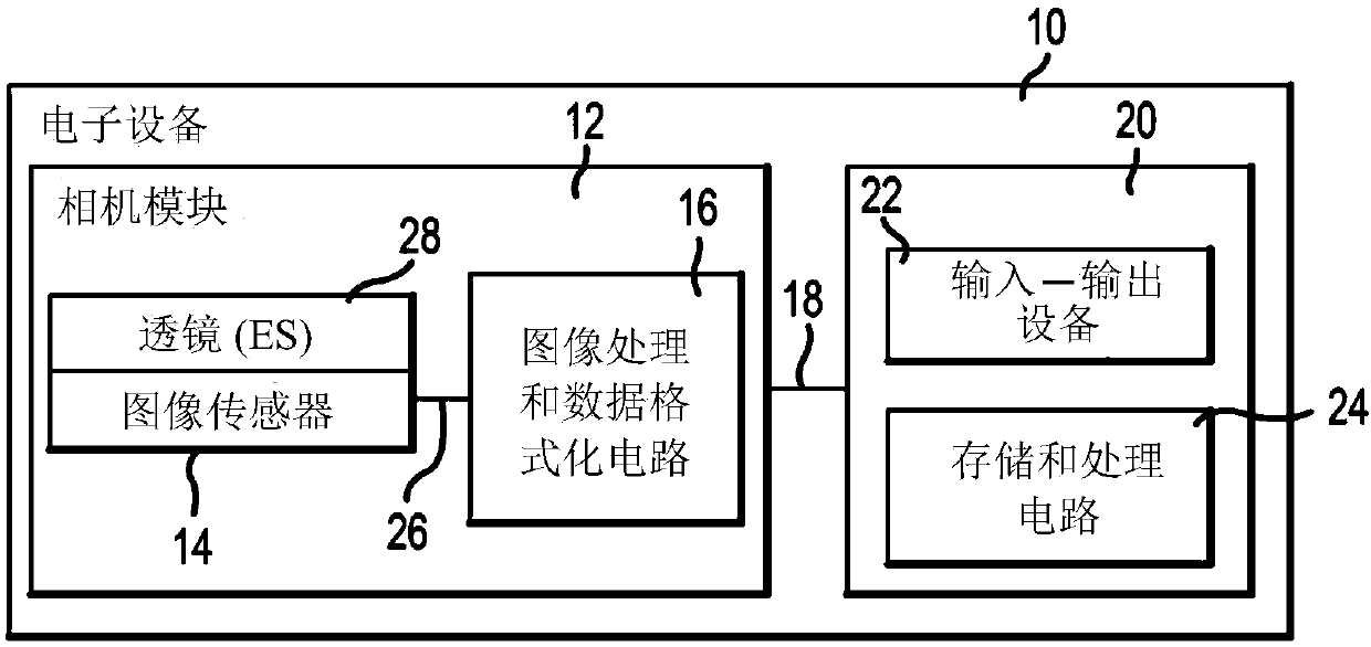
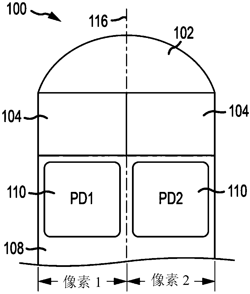
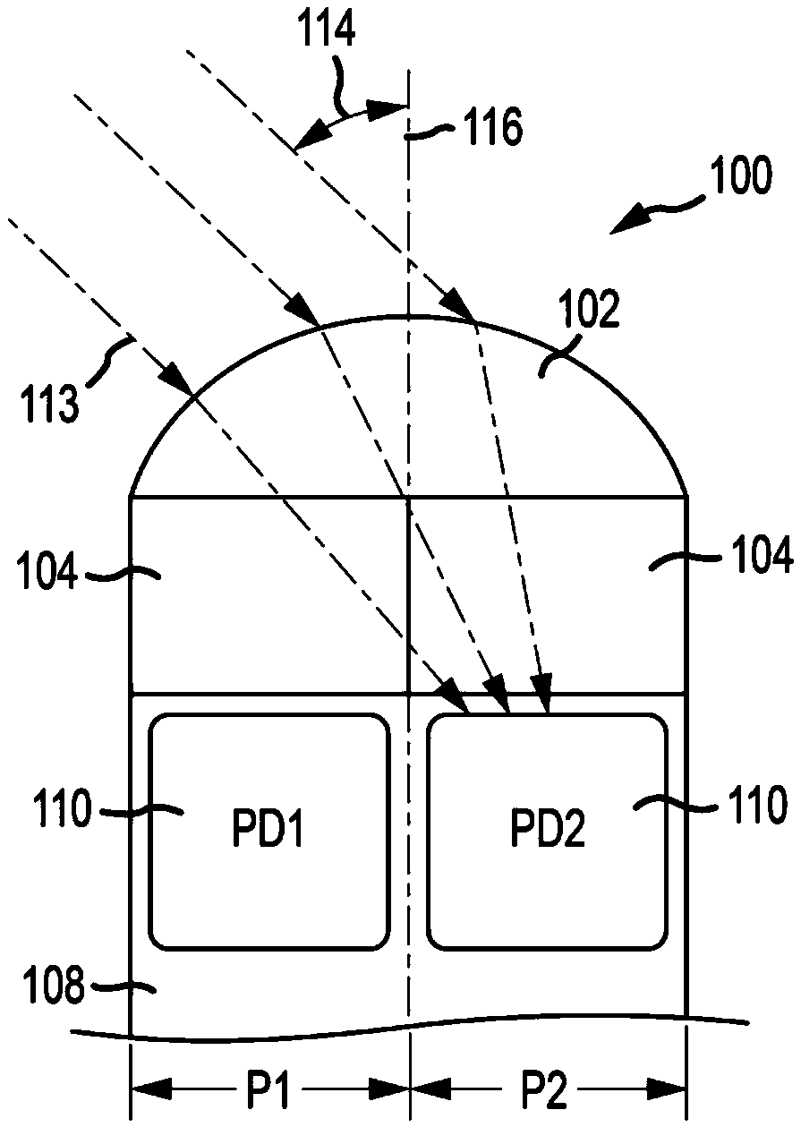
[0021] Embodiments of the present invention relate to image sensors with autofocus and depth sensing capabilities. figure 1 An electronic device with a camera module is shown in . Electronic device 10 may be a digital camera, computer, mobile phone, medical device, or other electronic device. Camera module 12 (sometimes referred to as an imaging device) may include one or more image sensors 14 and one or more lenses 28 . During operation, lens 28 (sometimes referred to as optics 28 ) focuses light onto image sensor 14 . Image sensor 14 includes photosensitive components (eg, pixels) that convert light into digital data. An image sensor can have any number (eg, hundreds, thousands, millions, or more) of pixels. A typical image sensor may, for example, have millions of pixels (eg, megapixels). For example, image sensor 14 may include bias circuits (e.g., source follower load circuits), sample and hold circuits, correlated double sampling (CDS) circuits, amplifier circuits, a...


PUM


Abstract

The invention relates to image sensors with calibrated phase detection pixels, and an operation method thereof. Image sensors may include phase detection pixels that are used to determine the distancebetween the image sensor and objects in a scene. To account for variations in the angular response of phase detection pixels across a pixel array, calibration may be performed. During calibration, animage sensor may take images of targets at known distances from the sensor. The known distances may be used to determine scaling factors that account for differences between the initially calculateddistances between the sensor and the targets and the actual distances between the sensor and the targets. The scaling factors may then be stored on the image sensor for future reference. During subsequent use of the image sensor, the image sensor may then obtain the appropriate scaling factor in real time for more accurate phase and distance determinations.

Description

technical field [0001] The present invention relates generally to imaging systems, and more particularly to imaging systems with phase detection capabilities. Background technique [0002] Modern electronic devices such as mobile phones, cameras and computers often use digital image sensors. Imaging sensors (sometimes referred to as imagers) may be formed from two-dimensional arrays of image sensing pixels. Each pixel receives incident photons (light) and converts these photons into electrical signals. Sometimes image sensors are designed to provide images to electronic devices using the Joint Photographic Experts Group (JPEG) format. [0003] Some applications such as autofocus and three-dimensional (3D) imaging may require electronic devices to provide stereo and / or depth sensing capabilities. For example, in order to bring an object of interest into focus in order to capture an image, the electronic device may need to identify the distance between the electronic device...

Claims


Application Information

Patent Timeline
Patent Type & Authority Applications(China)
IPC IPC(8): H04N17/00
CPCH04N17/002G06T3/4015H04N23/672H04N25/704G06T7/80G06T7/73G06T3/40G06T2207/10148G06T1/0007G06T7/571H04N23/67H04N25/75
Inventor 杜楠D·W·亚辛斯基
Owner SEMICON COMPONENTS IND LLC
Why Eureka
Try Eureka