Peripheral circuit structure of OLED display panel and OLED display panel

A peripheral circuit and display panel technology, applied in circuits, electrical components, electrical solid devices, etc., can solve the problems of increased frame width, different voltages, uneven brightness of display panels, etc., to improve display effects, reduce impedance voltage drop, Improve the effect of uneven brightness

Active Publication Date: 2019-07-09
WUHAN CHINA STAR OPTOELECTRONICS SEMICON DISPLAY TECH CO LTD
View PDF4 Cites 9 Cited by
  • Summary
  • Abstract
  • Description
  • Claims
  • Application Information

AI Technical Summary

Problems solved by technology

[0005] In the existing OLED display device, in order to provide the cathode with a low power supply voltage (VSS), a circle of cathode wiring is formed around the display area in the frame area of ​​the substrate. Sexual connection to receive the low voltage of the power supply from the driver chip, transmit it to the cathode, and drive the OLED in the display area to emit light. With the development of display technology, consumers have higher and higher requirements for the width of the border of the display screen. Frame and frameless display panels are gradually becoming the mainstream, and the impedance drop (IR drop) of the cathode traces in the frame area will cause the voltage of the cathode traces close to the driver chip to be different from the position far away from the driver chip. Leading to uneven brightness, the current common solution is to reduce the impedance by increasing the width of the cathode wiring or the thickness of the metal film layer, but this will lead to an increase in the frame width of the display panel, which does not meet the current narrow frame requirements, and the metal film layer is added The thickness conflicts with the existing process capability

Method used


Image

  • Peripheral circuit structure of OLED display panel and OLED display panel
  • Peripheral circuit structure of OLED display panel and OLED display panel
  • Peripheral circuit structure of OLED display panel and OLED display panel

Examples


Embodiment Construction

[0024] In order to further illustrate the technical means adopted by the present invention and its effects, the following describes in detail in conjunction with preferred embodiments of the present invention and accompanying drawings.

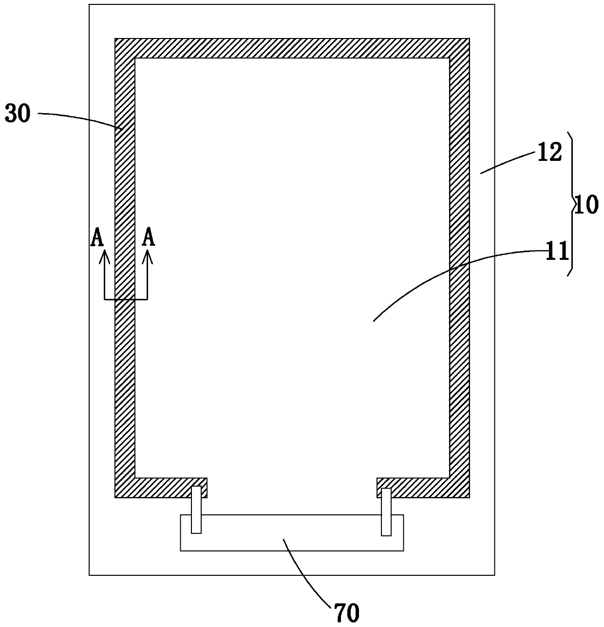
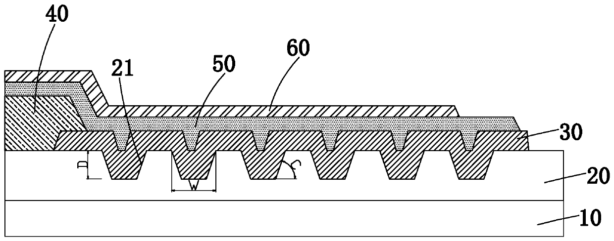
[0025] see Figure 1 to Figure 2 , the present invention provides a peripheral circuit structure of an OLED display panel, including a substrate 10, an insulating layer 20 disposed on the substrate 10, and a wiring 30 disposed on the insulating layer 20;

[0026] The substrate 10 includes a display area 11 and a frame area 12 surrounding the display area 11, the wiring 30 is located in the frame area 12, and the insulating layer 20 is separated from the area corresponding to the wiring 30 A plurality of grooves 21 are arranged, and the traces 30 fill the plurality of grooves 21 .

[0027] Specifically, the extending direction of the groove 21 is parallel to the extending direction of the wiring 30 , and the plurality of grooves 21 are arrange...


PUM


Abstract

The invention provides a peripheral circuit structure of an OLED display panel and an OLED display panel. The peripheral circuit structure of the OLED display panel comprises a substrate, an insulating layer arranged on the substrate and a wiring arranged on the insulating layer. The substrate comprises a display area and a border area surrounding the display area. The wiring is located in the border area. Multiple grooves arranged at intervals are formed in an area, corresponding to the wiring, of the insulating layer. The wiring fills the grooves. By arranging the grooves under the wiring and filling the grooves with the wiring, the cross-section area of the wiring can be increased, the IR drop of the wiring can be reduced, the display effect of the OLED display panel can be improved, and improvement can be made on the uneven brightness.

Description

technical field [0001] The invention relates to the field of display technology, in particular to a peripheral circuit structure of an OLED display panel and the OLED display panel. Background technique [0002] Organic light-emitting diode display devices have excellent characteristics such as self-illumination, no need for backlight, high contrast, thin thickness, wide viewing angle, fast response speed, flexible panels, wide operating temperature range, and simple structure and manufacturing process. It is considered as an emerging application technology for the next generation of flat panel displays. [0003] OLED display devices generally include: a substrate, an anode disposed on the substrate, a hole injection layer disposed on the anode, a hole transport layer disposed on the hole injection layer, a light emitting layer disposed on the hole transport layer, a device An electron transport layer on the light emitting layer, an electron injection layer on the electron ...

Claims


Application Information

Patent Timeline
Patent Type & Authority Applications(China)
IPC IPC(8): H01L27/32
CPCH10K59/1315
Inventor 崔耀晨
Owner WUHAN CHINA STAR OPTOELECTRONICS SEMICON DISPLAY TECH CO LTD
Why Eureka
Try Eureka