A kind of 3d NAND Flash

A unique, register group technology, applied in the field of 3D NAND Flash, can solve the problem of large bus consumption and power consumption, and achieve the effect of ensuring accuracy

Active Publication Date: 2021-10-22
INST OF MICROELECTRONICS CHINESE ACAD OF SCI
View PDF6 Cites 0 Cited by
  • Summary
  • Abstract
  • Description
  • Claims
  • Application Information

AI Technical Summary

Problems solved by technology

[0005] This application provides a kind of 3D NAND Flash, the purpose is to solve the problem that the power consumption of the bus in 3D NAND Flash is larger

Method used


Image

  • A kind of 3d NAND Flash
  • A kind of 3d NAND Flash
  • A kind of 3d NAND Flash

Examples


Embodiment Construction

[0034] The following will clearly and completely describe the technical solutions in the embodiments of the application with reference to the drawings in the embodiments of the application. Apparently, the described embodiments are only some of the embodiments of the application, not all of them. Based on the embodiments in this application, all other embodiments obtained by persons of ordinary skill in the art without making creative efforts belong to the scope of protection of this application.

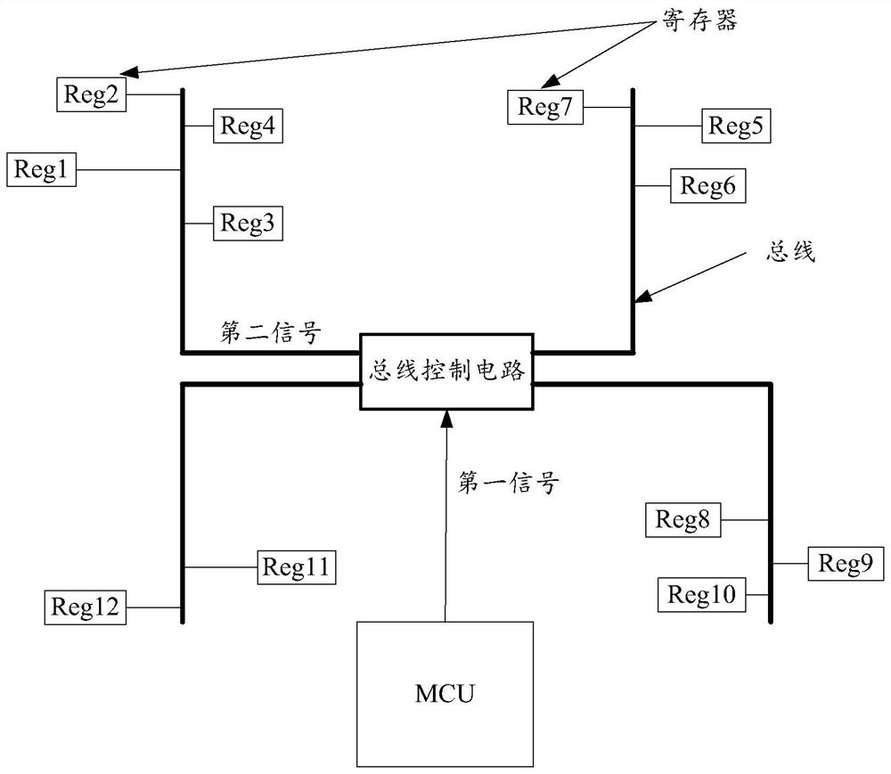
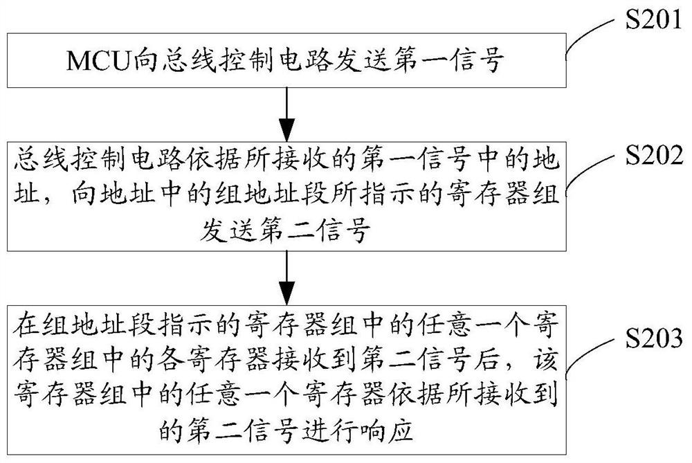
[0035] figure 1 A schematic diagram of a 3D NAND Flash provided for this application, including MCU, bus, bus control circuit and multiple registers. Wherein, the multiple registers are pre-divided into at least two register groups, so that any register group is connected to the bus control circuit through a part of the bus. For the convenience of description, a part of the bus is called a local bus, that is, any The register group is connected with the bus control circuit through ...


PUM


Abstract

This application discloses a 3D NAND Flash, including: MCU, bus control circuit, bus and multiple registers; multiple registers are pre-divided into at least two register groups; any register group has a preset unique group address segment, Any register has a preset unique local addressing address segment in the register group to which the register belongs; any register group is connected to the bus control circuit through the local bus; the bus control circuit is connected to the MCU; the MCU is used to control the bus The circuit sends a first signal; the first signal includes: the address of at least one register; the bus control circuit is used for sending the second register to the register in the register group indicated by the group address segment in the first signal after receiving the first signal Signal; the register in the register group indicated by the group address segment in the first signal is used to respond to the received second signal. Through the technical solution disclosed in this application, the power consumption of the bus can be reduced.

Description

technical field [0001] This application relates to the field of electronic information, in particular to a 3D NAND Flash. Background technique [0002] Flash is a non-volatile flash memory. Among them, 3D NAND Flash (three-dimensional NAND flash memory) is a kind of non-volatile flash memory. [0003] Currently, 3D NAND Flash includes a Microcontroller Unit (MCU), a bus, and multiple registers, wherein the MCU communicates with the registers through the bus so that the registers can store data specified by the MCU. [0004] However, the power consumption of the bus in 3D NAND Flash is relatively large. Contents of the invention [0005] The present application provides a 3D NAND Flash, aiming at solving the problem of high power consumption of the bus in the 3D NAND Flash. [0006] In order to achieve the above object, the application provides the following technical solutions: [0007] This application provides a 3D NAND Flash, including: MCU, bus control circuit, bus...

Claims


Application Information

Patent Timeline
Patent Type & Authority Patents(China)
IPC IPC(8): G06F12/02
CPCG06F12/0246Y02D10/00
Inventor 高帅侯旭王颀霍宗亮叶甜春
Owner INST OF MICROELECTRONICS CHINESE ACAD OF SCI
Why Eureka
Try Eureka