Check patentability & draft patents in minutes with Patsnap Eureka AI!

Array substrate and preparation method thereof

A technology for an array substrate and a base substrate, which is applied to the field of array substrates and their preparation, can solve the problems of complex ion implantation process and other problems, and achieve the effect of reducing the ion implantation process and alleviating the complexity of the ion implantation process.

Active Publication Date: 2019-07-23
WUHAN CHINA STAR OPTOELECTRONICS TECH CO LTD
View PDF7 Cites 1 Cited by
  • Summary
  • Abstract
  • Description
  • Claims
  • Application Information

AI Technical Summary

Problems solved by technology

[0005] The invention provides a method for preparing an array substrate to solve the problem of complex ion implantation process in the existing array substrate

Method used


Image

  • Array substrate and preparation method thereof
  • Array substrate and preparation method thereof
  • Array substrate and preparation method thereof

Examples


preparation example Construction

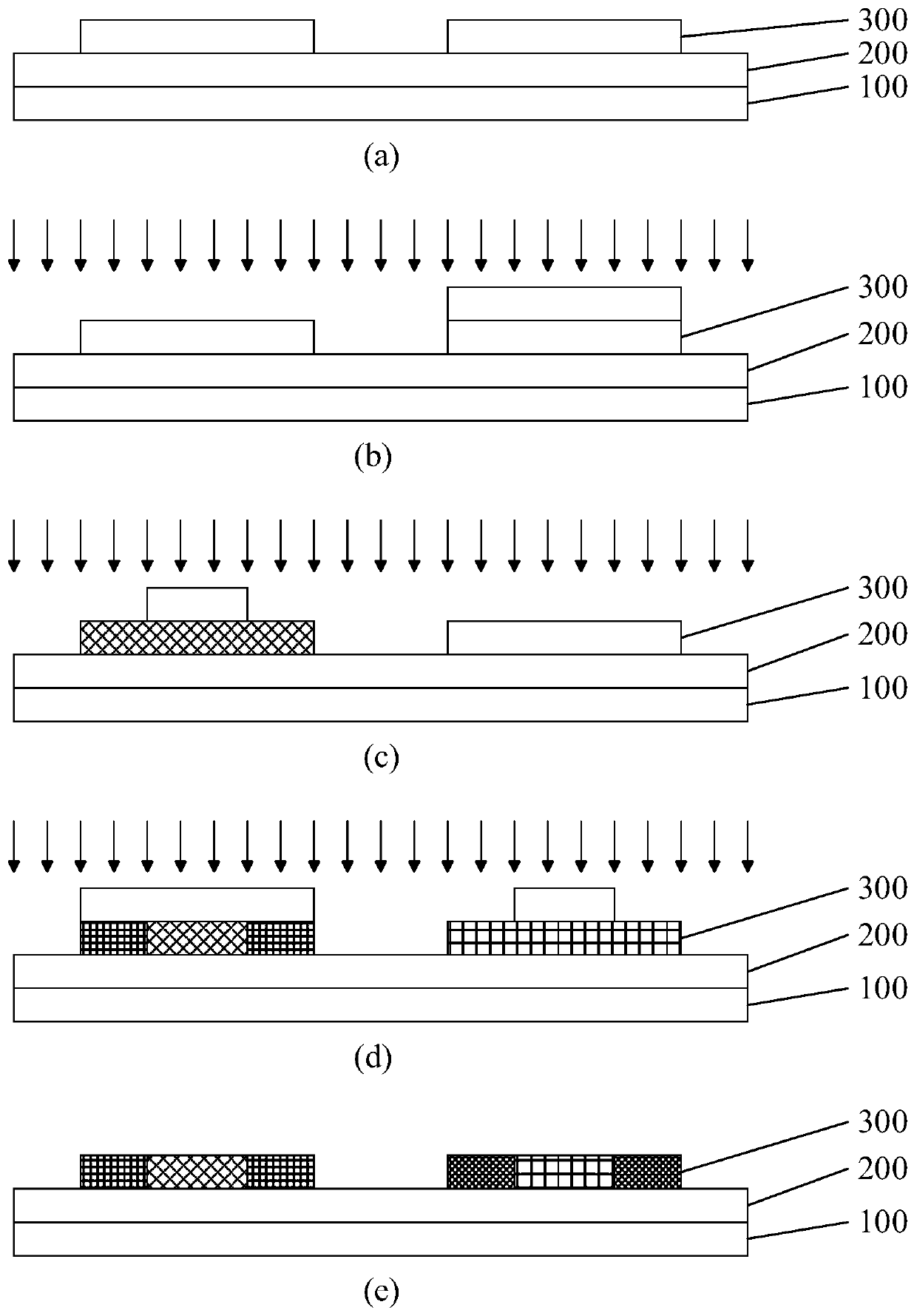
[0030] Aiming at the problems of complex ion implantation process and high production cost in the existing array substrate, the present invention provides a preparation method of the array substrate to alleviate this problem.

[0031] In one embodiment, as figure 2 As shown, the steps of the preparation method of the array substrate provided by the present invention include:

[0032] S1. Provide a base substrate, on which a first polysilicon layer corresponding to a first type thin film transistor and a second polysilicon layer corresponding to a second type thin film transistor are prepared, the first polysilicon layer The crystalline silicon layer and the second polysilicon layer are arranged in the same layer;

[0033] S2. Prepare a photoresist layer on the polysilicon layer, the thickness of the photoresist layer corresponding to the gate region of the second type thin film transistor is greater than the thickness of the photoresist layer in other regions;

[0034] S3. ...


PUM


Abstract

The invention provides an array substrate and a preparation method thereof. The preparation method comprises the following steps of providing a base substrate, and preparing a first polysilicon layercorresponding to a first type thin film transistor and a second polysilicon layer corresponding to a second type thin film transistor on the base substrate; forming photoresist layers on the polysilicon layers, wherein the thickness of the photoresist layers corresponding to the gate region of the second type thin film transistor is larger than that of the photoresist layers in the remaining regions; performing first ion doping on the polysilicon layers; processing the photoresist layers, thinning and remaining the photoresist layers of the corresponding region of the gate of the first type thin film transistor, and stripping the photoresist layers of the remaining regions; performing second ion doping on the polysilicon layers; and stripping the remaining photoresist layers. The array substrate and preparation method thereof provided by the invention, by preparing the photoresist layers with different thicknesses for different ion implantation regions, can complete the implantation ofthe first ions and the second ions by one ion implantation process, thereby reducing the ion implantation process and alleviating the problem that the ion implantation process is complicated and theproduction cost is high existing in the current array substrate.

Description

technical field [0001] The invention relates to the field of display manufacturing process, in particular to an array substrate and a preparation method thereof. Background technique [0002] TFT (Thin Film Transistor, Thin Film Transistor) array substrate is the main component in current LCD devices and OLED devices, and its performance is directly related to the performance of the display device. LTPS (Low temperature poly-silicon, low-temperature polysilicon), due to its high electron mobility, is widely used in the production of small and medium-sized high-resolution LCD and OLED display panels. In order to meet the development of high-end products, the TFT driving circuit of the LTPS panel mostly adopts CMOS (Complementary Metal Oxide Semiconductor, Complementary Metal Oxide Semiconductor) driving. [0003] Such as figure 1 Shown, the preparation method of existing CMOS array substrate comprises preparation polysilicon active layer, and its concrete steps comprise: as...

Claims


Application Information

Patent Timeline
Patent Type & Authority Applications(China)
IPC IPC(8): H01L21/77H01L21/266H01L27/12
CPCH01L21/266H01L27/127H01L27/1288
Inventor 李继禄
Owner WUHAN CHINA STAR OPTOELECTRONICS TECH CO LTD
Features
  • R&D
  • Intellectual Property
  • Life Sciences
  • Materials
  • Tech Scout
  • Unparalleled Data Quality
  • Higher Quality Content
  • 60% Fewer Hallucinations
Learn More