Check patentability & draft patents in minutes with Patsnap Eureka AI!

Semiconductor memory comprising pads arranged in parallel

A memory and semiconductor technology, used in semiconductor devices, semiconductor/solid-state device components, static memory, etc., to solve problems such as increased power consumption by interconnect lines and reduced signal integrity

Pending Publication Date: 2019-07-26
SAMSUNG ELECTRONICS CO LTD
View PDF0 Cites 1 Cited by
  • Summary
  • Abstract
  • Description
  • Claims
  • Application Information

AI Technical Summary

Problems solved by technology

[0005] As the length of the back-end interconnect increases, the power consumed by the back-end interconnect increases and the signal integrity (SI) of the signal transmitted through the back-end interconnect decreases

Method used


Image

  • Semiconductor memory comprising pads arranged in parallel
  • Semiconductor memory comprising pads arranged in parallel
  • Semiconductor memory comprising pads arranged in parallel

Examples


Embodiment Construction

[0021] Example embodiments provide a semiconductor memory for reducing power consumption and improving signal integrity.

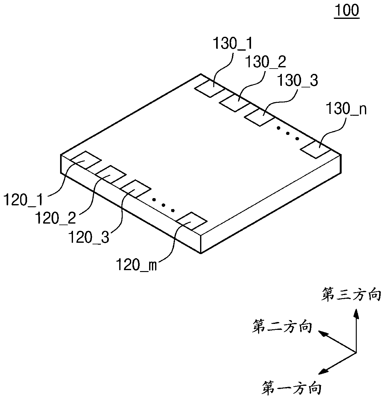
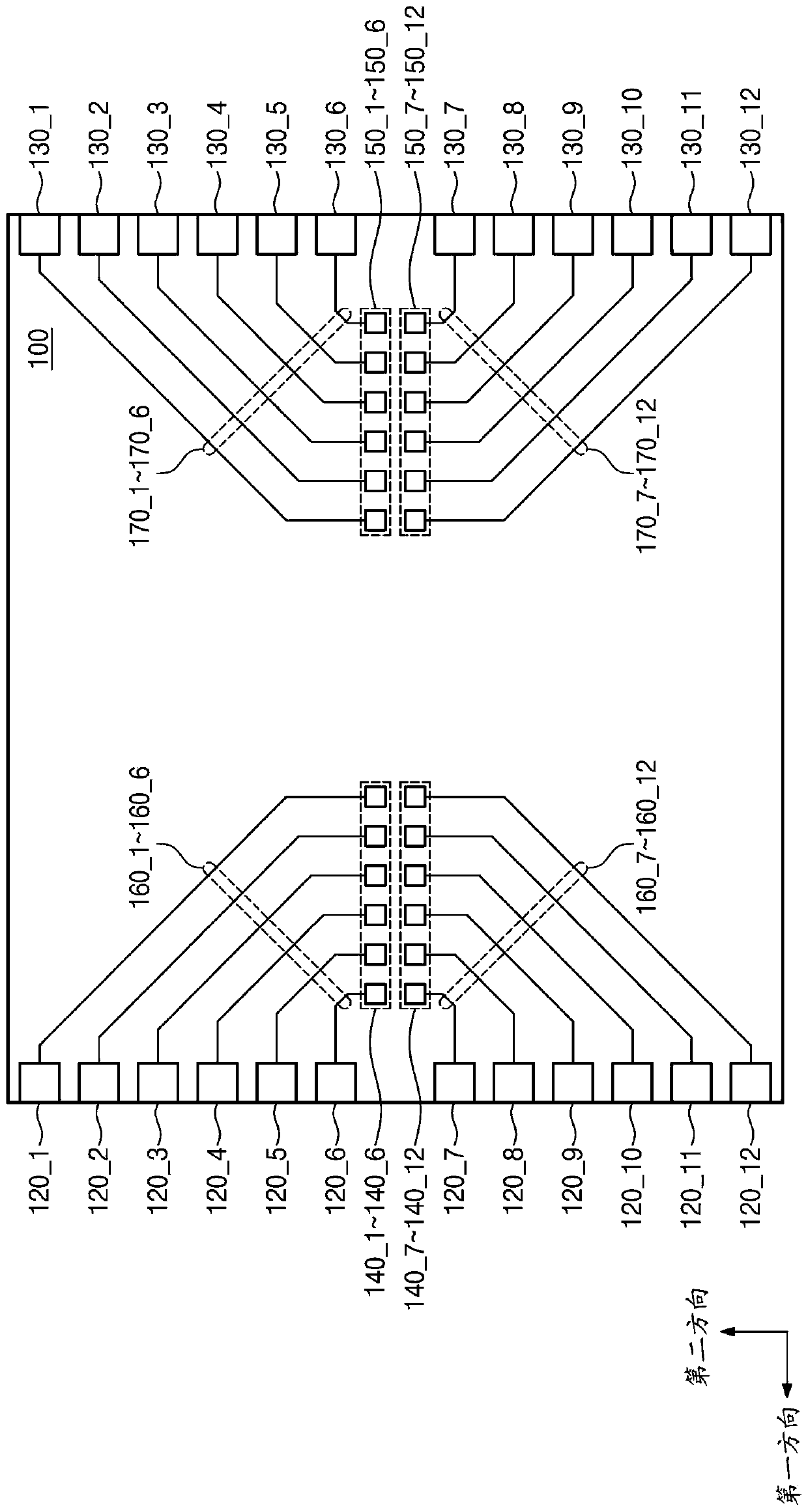
[0022] figure 1 is a perspective view of a semiconductor memory 100 according to an example embodiment. Illustratively, the shape of the die of semiconductor memory 100 is figure 1 shown in . figure 1 The upper surface of the semiconductor memory 100 shown in may be the back end of the die of the semiconductor memory 100 . refer to figure 1 , first external pads 120_1 to 120_m (m: an integer greater than 1) and second external pads 130_1 to 130_n (n: an integer greater than 1) may be disposed on the back end of the semiconductor memory 100 .

[0023] The first external pads 120_1 to 120_m may be disposed on a side of the rear end facing the first direction. The second external pads 130_1 to 130_n may be disposed on a side of the rear end facing a direction opposite to the first direction. The first external pads 120_1 to 120_m and the second external...


PUM


Abstract

A semiconductor memory includes a plurality of first pads arranged in a first direction, a plurality of second pads arranged parallel to the plurality of first pads and in the first direction, a plurality of third pads arranged in a second direction perpendicular to the first direction, and a plurality of fourth pads arranged in the second direction. The semiconductor memory further includes firstinterconnection wires extending from the plurality of first pads in the second direction, the first interconnection wires being connected to the plurality of third pads, and second interconnection wires extending from the plurality of second pads in an opposite direction to the second direction, the second interconnection wires being connected to the plurality of fourth pads.

Description

technical field [0001] Devices consistent with example embodiments relate to a semiconductor circuit, and more particularly, to a semiconductor memory including pads arranged in parallel. Background technique [0002] Semiconductor memories are manufactured through a number of processes. The plurality of fabrication processes includes processes of depositing or etching insulating, conducting, or semiconducting materials. When the die of the semiconductor memory is fully fabricated, the internal pads, external pads, and back-end interconnect lines are exposed on the back-end of the semiconductor memory. [0003] The internal pads are connected to various components fabricated within the die of the semiconductor memory. The location of the internal pads may be determined according to the arrangement or configuration of elements within the die of the semiconductor memory. The external pads are formed at positions where they are easily connected with the semiconductor package...

Claims


Application Information

Patent Timeline
IPC IPC(8): H01L23/488H01L23/52G11C5/06
CPCH01L23/488H01L23/52G11C5/063G11C5/025G11C5/04G11C2207/105H01L2224/02379H01L24/02H01L2224/02375H01L2224/04042H01L2224/06154H01L24/06H01L2924/1434G11C7/1084G11C5/06H01L2224/06158G11C8/10
Inventor 孙永训金始弘吴台荣河庆洙
Owner SAMSUNG ELECTRONICS CO LTD
Features
  • R&D
  • Intellectual Property
  • Life Sciences
  • Materials
  • Tech Scout
  • Unparalleled Data Quality
  • Higher Quality Content
  • 60% Fewer Hallucinations
Learn More