Supercharge Your Innovation With Domain-Expert AI Agents!

PCB component detection method based on deep learning

A PCB board and deep learning technology, applied in the direction of neural learning methods, instruments, computer components, etc., can solve the problems of low degree of automation, lack, single function, etc., and achieve the effect of solving docking difficulties

Active Publication Date: 2019-07-30
NANJING UNIV OF POSTS & TELECOMM
View PDF3 Cites 19 Cited by
  • Summary
  • Abstract
  • Description
  • Claims
  • Application Information

AI Technical Summary

Problems solved by technology

[0003] In recent years, as the size of the components on the PCB becomes smaller and there are many types, the pure manual visual inspection method can no longer meet the needs of production in terms of accuracy and speed. Automatically monitor the appearance, type, position, polarity, model and other indicators of components on the PCB
Most of the traditional visual inspection methods rely on worktables, robotic arms, CCD lenses, etc. to compare and analyze standard images. This method is slow and the degree of automation is not high.
With the vigorous development of deep learning, more target detection methods based on neural networks have become a popular research direction for PCB board detection. This method is fast and accurate. At the same time, it can realize an end-to-end detection solution with a relatively high degree of automation. However, the function is relatively single, and most of them only detect the position and category of components and lack a highly integrated and comprehensive automatic detection system, including the detection of polarity, model and other information of components.

Method used


Image

  • PCB component detection method based on deep learning
  • PCB component detection method based on deep learning
  • PCB component detection method based on deep learning

Examples


Embodiment

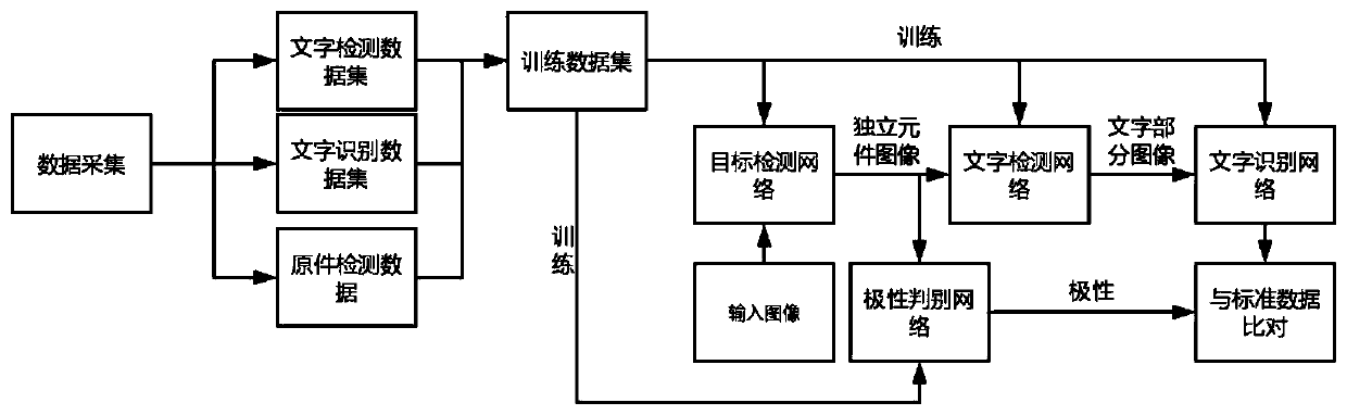
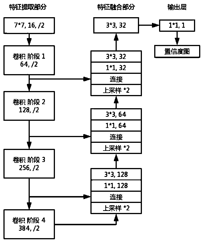
[0038] This embodiment provides a PCB component detection method based on deep learning, such as figure 1 As shown, the specific steps are:

[0039] (1) Prepare the data set:

[0040] Take a large number of sample images of PCB boards. Considering that the direction and angle of each component symbol are different, it is necessary to set up four cameras in different directions to collect image information in different directions. Since the image angle taken is not conducive to image detection and text recognition, image correction must be performed. In order to improve the correction accuracy, you can choose to use the marker method to estimate the pose of the camera. Set four markers at fixed positions, binarize the image, use edge detection to detect the outline and corner coordinates of the marker, perform radial transformation and perspective transformation according to the corner coordinates to obtain the corrected standard image, and use labelme to correct the image La...


PUM


Abstract

The invention discloses a PCB component detection method based on deep learning. The method comprises the steps of obtaining a large number of PCB images and marking the PCB images for training a network; training faster-rcnn for detecting the position of a component and cutting the component; training a simple convolutional network to judge the polarity of the component; training an EAST networkto detect the position of a textbox on the component image and cutting the textbox; training the CRNN network to identify the text content in the cut textbox image; and comparing the polarity and thetext content with a PCB design file to obtain a result. According to the invention, full-automatic identification of the object identifier is realized, and the problem of difficult docking of each detection stage at present is solved.

Description

technical field [0001] The invention relates to the technical field of automatic detection of PCB components, in particular to a method for detecting PCB components based on deep learning. Background technique [0002] PCB, or printed circuit board, is an important part of various electronic devices and a support for electronic components. It is used in almost every electronic device in our daily life, such as electronic watches, calculators, computers, and electronic communications. PCB version. The reason why the PCB board can get more and more extensive development is inseparable from its high reliability and high density characteristics. These characteristics also determine that it has very high requirements for the accuracy of each component, so the scale of the PCB board Chemical testing has become one of the important processes of PCB board production. [0003] In recent years, as the size of the components on the PCB becomes smaller and there are many types, the pu...

Claims


Application Information

Patent Timeline
IPC IPC(8): G06T7/00G06T7/11G06T7/13G06K9/20G06K9/32G06K9/62G06N3/04G06N3/08
CPCG06T7/0004G06T7/11G06T7/13G06N3/084G06T2207/30141G06V10/22G06V20/63G06V30/10G06N3/045G06F18/2414Y02P90/30
Inventor 高浩杨泽宇胡海东
Owner NANJING UNIV OF POSTS & TELECOMM
Features
  • R&D
  • Intellectual Property
  • Life Sciences
  • Materials
  • Tech Scout
  • Unparalleled Data Quality
  • Higher Quality Content
  • 60% Fewer Hallucinations
Learn More