Transfer device and manufacturing method of display substrate

A technology for transferring devices and display substrates, which is applied in semiconductor/solid-state device manufacturing, electrical components, electric solid-state devices, etc. It can solve the problems of low manufacturing yield of display substrates, achieve the effect of simplifying the manufacturing process and improving the manufacturing yield

Inactive Publication Date: 2019-08-06
BOE TECH GRP CO LTD +1
View PDF15 Cites 6 Cited by
  • Summary
  • Abstract
  • Description
  • Claims
  • Application Information

AI Technical Summary

Problems solved by technology

[0003] The embodiment of the present invention provides a transfer device and a method for manufacturing a display substrate, so as to solve the problem of low manufacturing yield of the existing method for manufacturing a display substrate

Method used


Image

  • Transfer device and manufacturing method of display substrate
  • Transfer device and manufacturing method of display substrate
  • Transfer device and manufacturing method of display substrate

Examples


Embodiment Construction

[0035] In order to make the technical problems, technical solutions and advantages to be solved by the present invention clearer, the following will describe in detail with reference to the drawings and specific embodiments.

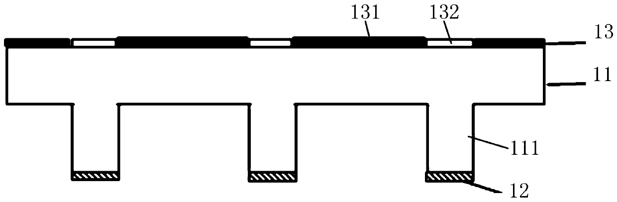
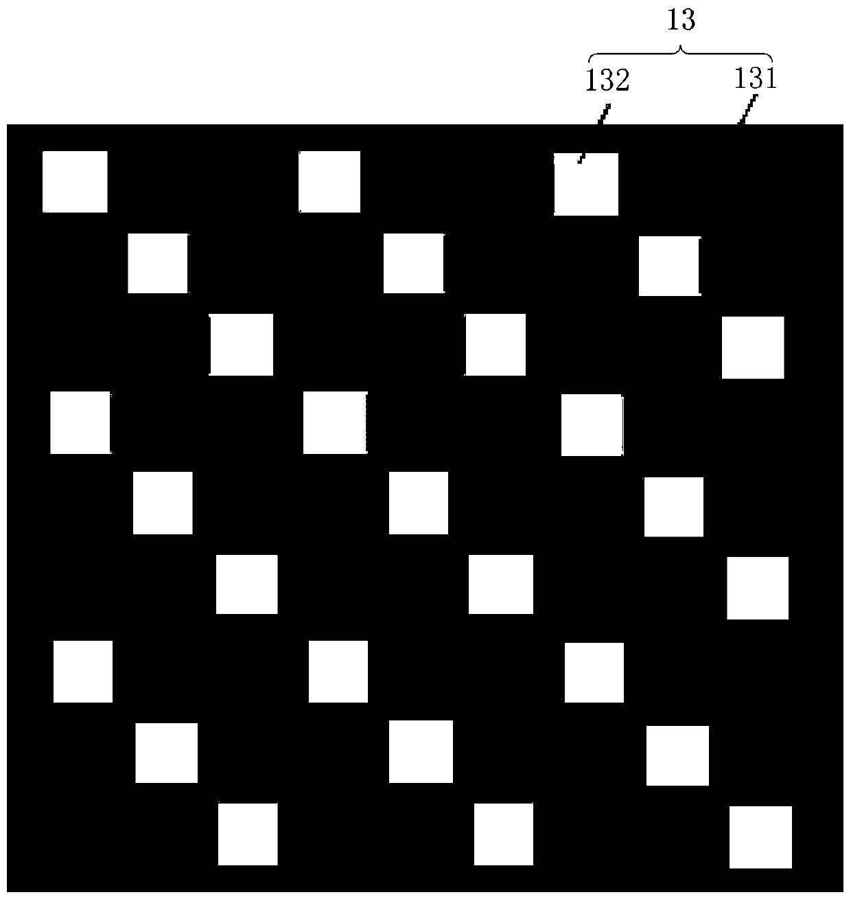
[0036] see figure 1 , the embodiment of the present invention provides a transfer device 1, comprising: a transparent carrier 11; one side surface of the transparent carrier 11 is provided with a plurality of adhesive parts 12 arranged at intervals, and the adhesive parts 12 adopt photosensitive Adhesive material; the other side surface of the transparent carrier 11 is provided with a plurality of opaque patterns 131, and the orthographic projection of the gap between the opaque patterns 131 on the transparent carrier 11 is related to the adhesive portion The orthographic projections of 12 on the transparent carrier 11 overlap.

[0037] In the embodiment of the present invention, the adhesive part 12 is a photosensitive adhesive material. When the adhes...


PUM


Abstract

The embodiment of the invention provides a transfer device and a manufacturing method of a display substrate. The transfer device comprises a transparent carrier. Multiple adhesion parts distributed at intervals are arranged on the surface of one side of the transparent carrier, and the adhesion parts are made of a photosensitive viscous material. Through the transfer device provided by the embodiment of the invention, the manufacturing process of the display substrate can be simplified, and the manufacturing yield can be improved.

Description

technical field [0001] The invention relates to the technical field of liquid crystal display, in particular to a transfer device and a manufacturing method of a display substrate. Background technique [0002] In the process of making Micro LED (light-emitting diode) chips into display devices, it is usually necessary to transfer a large number (millions) of Micro LED chips to the driving substrate to form an LED array. Due to the small size of Micro LED chips, it is difficult to accurately align them. , During the transfer process, it is easy to fail to successfully connect with the driving substrate, resulting in dead pixels and reducing the manufacturing yield. Contents of the invention [0003] Embodiments of the present invention provide a transfer device and a method for manufacturing a display substrate, so as to solve the problem of low manufacturing yield of the existing method for manufacturing a display substrate. [0004] In a first aspect, an embodiment of t...

Claims


Application Information

Patent Timeline
Patent Type & Authority Applications(China)
IPC IPC(8): H01L33/00H01L21/67H01L25/075
CPCH01L21/67132H01L25/0753H01L33/0095
Inventor 查长军刘超彭元鸿曾娅魏雄周黎敏
Owner BOE TECH GRP CO LTD
Why Eureka
Try Eureka